ZHCU837 December 2021
- 说明
- 资源
- 特性
- 应用
- 5
- 1System Description
-
2System Overview
- 2.1 Block Diagram
- 2.2 Highlighted Products
- 2.3
Design Considerations
- 2.3.1
Design Hardware Implementation
- 2.3.1.1 Hall-Effect Switches
- 2.3.1.2 Linear Hall-Effect Sensor Output
- 2.3.1.3 Power Supply
- 2.3.1.4 Transistor Circuit for Creating High-Voltage Enable Signal
- 2.3.2 Alternative Implementations
- 2.3.1
Design Hardware Implementation
- 3Hardware, Software, Testing Requirements, and Test Results
- 4Design and Documentation Support
2.3.1.1.4.1 Placement of U1 and U2 Sensors
The following procedure was used to find the placement of U1 and U2:
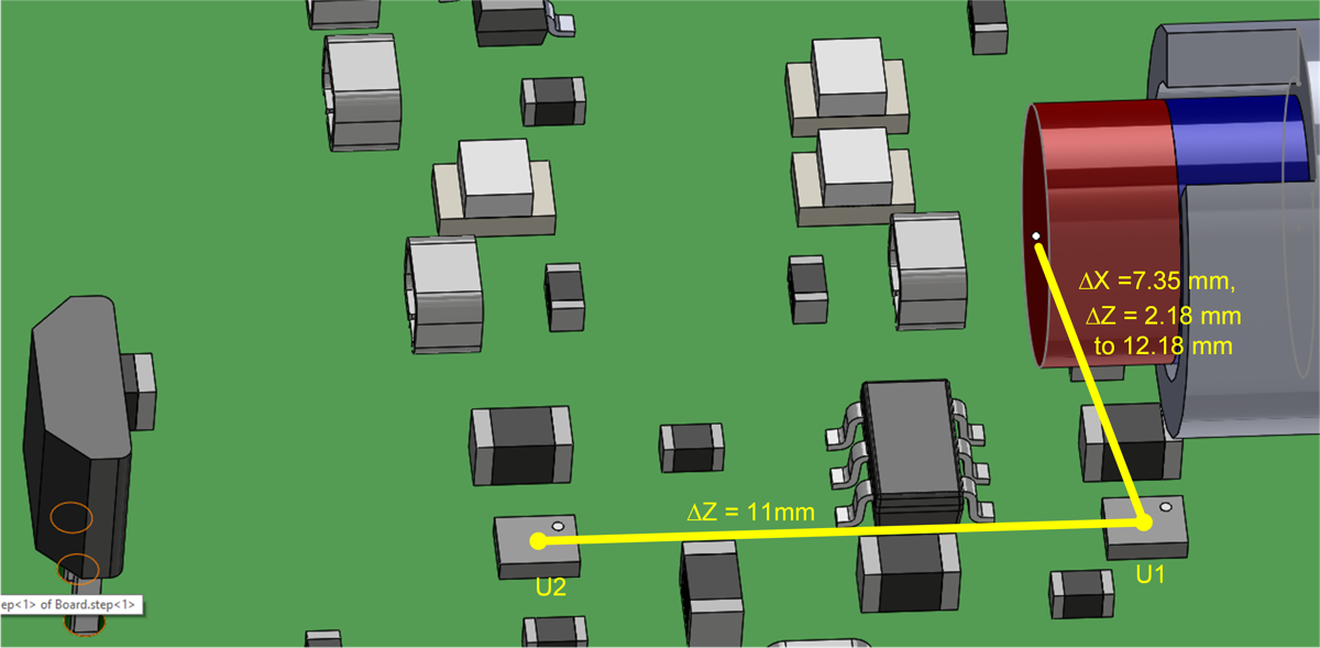
- An initial y-component displacement of 0 mm was selected for switches U1 and U2. In the view shown in Figure 2-14, switch U1 cannot be seen because it is underneath the magnet. Figure 2-15 shows a rotated and zoomed in version of Figure 2-14, which better shows U1. The white dot at the left face of the magnet is the center-point on the surface of the left face of the magnet. Both U1 and U2 are placed so that the sensing element within these devices have no y-direction displacement from the white dot at the magnet.
 Figure 2-15 Zoomed and Rotated View of Board Within 3D Printed Trigger Module
 - An initial x-component displacement was selected for the distance from the dot on the magnet to U1 and U2. Since U1 and U2 cannot be moved in the x direction due to being surface mount parts with fixed heights, changing the x-component displacement involves moving the magnet in the x direction or putting U1 and U2 on the opposite layer of the PCB. If the magnet is moved in the x direction, note that the impact of this change on the DRV5056 output must be verified if the height of the DRV5056 through-hole package cannot be adjusted accordingly.
- The z-component displacement from U1 to the dot on the magnet was selected. To ensure a more robust design, place U1, which only reacts to a positive field, so that the magnetic field at U1 in the off position is slightly negative. The rest state magnetic field is made slightly negative by slightly displacing U1 in the z direction so that the sensing element is under the north pole of the magnet.
- After the z component of U1 was selected, a simulation was done to verify that the sensed magnetic flux density of the sensor was less than BRP when the trigger was at rest. In addition, the sensed magnetic flux density must be greater than BOP for a trigger displacement value of dmin to dmax, where dmin is the desired trigger displacement at which the system is waked up and dmax is the largest trigger displacement distance (10 mm for this design). If these conditions are not met, take the following actions:
- Restart from step 3 with a different z-component displacement.
- Restart from step 2 with a different x-component displacement. Note that the impact of this change on the DRV5056 output must be verified if the height of the DRV5056 through-hole package cannot be adjusted accordingly.
- Modify the dimensions or material of the magnet and restart from step 2. Note that the impact of this change on the DRV5056 output must be verified.
- The z-component displacement from U2 to the dot on the magnet was selected.
- After the z component of U2 was selected, a simulation was done to verify that the sensed magnetic flux density of the sensor was less than BOP during the entire trigger displacement range. If these conditions are not met, take the following actions:
- Restart from step 5 with a different z-component displacement.
- Restart from step 2 with a different x-component displacement. Note that the impact of this change on the DRV5056 output must be verified if the height of the DRV5056 through-hole package cannot be adjusted accordingly.
- Modify the dimensions or material of the magnet and restart from step 2 again. Note that the impact of this change on the DRV5056 output must be verified.
Based on implementing the previous procedures, the following distances were obtained and used for this design:
- U1 distance components
- X-component displacements
- X-component from top of package to white dot of magnet = 7.35 mm
- X-component (“sensor z-offset” parameter in tool) from top of package to bottom of magnet = 7.35 – magnet radius = 4.96875
- X-component (sensor z-offset in tool) from sensing element to bottom of magnet to sensing element = 4.96875 + 0.150 = 5.11875 mm
- Y-component displacement = 0 mm
- Z-component displacement
- Trigger not pressed
- Z-component from sensing element to white dot of magnet (d1 in tool) = 2.18 mm
- Z-component from sensing element to magnet center = 2.18 – 0.5 × magnet thickness = 2.18 – 0.5(4.76) = –0.2 mm
- Maximum trigger displacement = 10 mm
- Z-component from sensing element to white dot of (d2 in tool) = 12.18 mm
- Z-component from sensing element to magnet = 12.18 – 0.5 × magnet thickness) = 12.18 – 0.5(4.76) = 9.8 mm
- Trigger not pressed
- X-component displacements
U2 distance components
- X-component displacement = x-component displacement of U1
- Y-component displacement = y-component displacement of U1
- Z-component displacement
- Z-component displacement from U1 sensing element to U2 sensing element = 11 mm
- Trigger not pressed
- Z-component from sensing element to white dot of magnet = –8.82 mm
- Z-component from sensing element to magnet center = –8.82 – 0.5 × magnet thickness = –8.82 – 0.5(4.76) = –11.2 mm
Maximum trigger displacement = 10 mm
- Z-component from sensing element to white dot of Figure 2-15 = 1.18 mm
- Z-component from sensing element to magnet = 1.18 – 0.5 × magnet thickness) = 1.18 – 0.5(4.76) = –1.2 mm