ZHCU837 December 2021
- 说明
- 资源
- 特性
- 应用
- 5
- 1System Description
-
2System Overview
- 2.1 Block Diagram
- 2.2 Highlighted Products
- 2.3
Design Considerations
- 2.3.1
Design Hardware Implementation
- 2.3.1.1 Hall-Effect Switches
- 2.3.1.2 Linear Hall-Effect Sensor Output
- 2.3.1.3 Power Supply
- 2.3.1.4 Transistor Circuit for Creating High-Voltage Enable Signal
- 2.3.2 Alternative Implementations
- 2.3.1
Design Hardware Implementation
- 3Hardware, Software, Testing Requirements, and Test Results
- 4Design and Documentation Support
2.3.1.4 Transistor Circuit for Creating High-Voltage Enable Signal
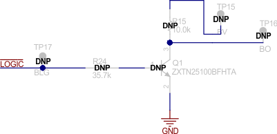
The design has an optional transistor circuit (shown in Figure 2-27) that can be used for creating a high-voltage signal that provides information on whether the system is in sleep or wake mode. This circuit takes the active-low output signal from the SN74HCS00 logic gate and produces an active-high, high-voltage version of this signal.
 Figure 2-27 Transistor Circuit
The circuit in Figure 2-27 was added in case it is desired to emulate connecting or disconnecting the battery from a signal based on the sleep state. This signal can be used to put an external system to sleep if that external system goes to sleep mode based on the state of a high-voltage pin.
To use this circuit, populate R24, Q1, and R15. Next, apply the high-voltage input on the BV test point. This high-voltage input is the voltage that the output enable signal should be referenced with respect to. As an example, connect this high-voltage input to the power drill battery to create an enable signal that is referenced with respect to the battery in the drill. The output signal is produced on the BO test point. If the system is in sleep mode, the voltage at BO is equal to 0 V. If the system is in active mode, the voltage at BO is set to the voltage applied at BV.
The circuit in Figure 2-27 is mainly for demonstration purposes. To reduce system current consumption, note that circuit is not populated by default. Also note that the produced enable signal is not meant to power a drill or any other system. The signal is primarily intended to trigger other components that actually connect or disconnect power to the system, such as an external high current eFuse, load switch, or hot-swap controller.