ZHCU837 December 2021
- 说明
- 资源
- 特性
- 应用
- 5
- 1System Description
-
2System Overview
- 2.1 Block Diagram
- 2.2 Highlighted Products
- 2.3
Design Considerations
- 2.3.1
Design Hardware Implementation
- 2.3.1.1 Hall-Effect Switches
- 2.3.1.2 Linear Hall-Effect Sensor Output
- 2.3.1.3 Power Supply
- 2.3.1.4 Transistor Circuit for Creating High-Voltage Enable Signal
- 2.3.2 Alternative Implementations
- 2.3.1
Design Hardware Implementation
- 3Hardware, Software, Testing Requirements, and Test Results
- 4Design and Documentation Support
2.3.1.1.4 Hall Switch Placement
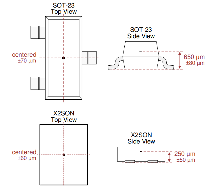
The magnetic flux density detected by a Hall sensor is dependent on the magnet dimensions, magnet material, and the distance from the magnet to the sensing element within the Hall sensor. Note that the location of the sensing element varies for each package of the DRV5032. Figure 2-13 shows the location of the sensing element in the X2SON and SOT-23 packages of the DRV5032. The two pictures on the right express the sensing location with respect to the bottom of the X2SON and SOT-23 packages of the DRV5032. To express the sensing location so that it is with respect to the top of a package, subtract the readings that are with respect to the bottom of the package from the package height. As an example, if the X2SON package height is 400 μm and the distance from the bottom of the package to the sensing element is 250 μm, the distance from the top of the X2SON package to the sensing element is 400 – 250 = 150 μm. Similarly, if the SOT-23 height is 1120 μm and the distance from the bottom of the package to the sensing element is 650 μm, the distance from the top of the SOT-23 package to the sensing element is 1120 – 650 = 470 μm.
 Figure 2-13 Location of Sensing Element Within X2SON and SOT-23 Packages of DRV5032
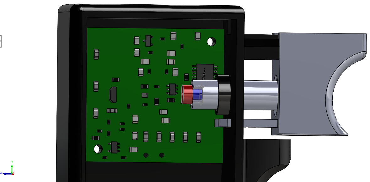
Based on the magnet specifications and the distance from the magnet to the sensing elements, simulations were done to estimate the expected sensed magnetic flux density at each sensor across the trigger displacement range. For detailing the distances from the magnet to the Hall sensors, the convention shown in Figure 2-14 was used. In this figure, the z-axis is defined as going from right to left (this is the direction of the trigger movement), the y-axis is defined as going from up to down, and the x direction is defined as going into the page (from the top layer of the PCB to the bottom layer of the PCB).
 Figure 2-14 Board Picture Within 3D Printed Trigger Module