ZHCU837 December 2021
- 说明
- 资源
- 特性
- 应用
- 5
- 1System Description
-
2System Overview
- 2.1 Block Diagram
- 2.2 Highlighted Products
- 2.3
Design Considerations
- 2.3.1
Design Hardware Implementation
- 2.3.1.1 Hall-Effect Switches
- 2.3.1.2 Linear Hall-Effect Sensor Output
- 2.3.1.3 Power Supply
- 2.3.1.4 Transistor Circuit for Creating High-Voltage Enable Signal
- 2.3.2 Alternative Implementations
- 2.3.1
Design Hardware Implementation
- 3Hardware, Software, Testing Requirements, and Test Results
- 4Design and Documentation Support
2.3.1.1 Hall-Effect Switches
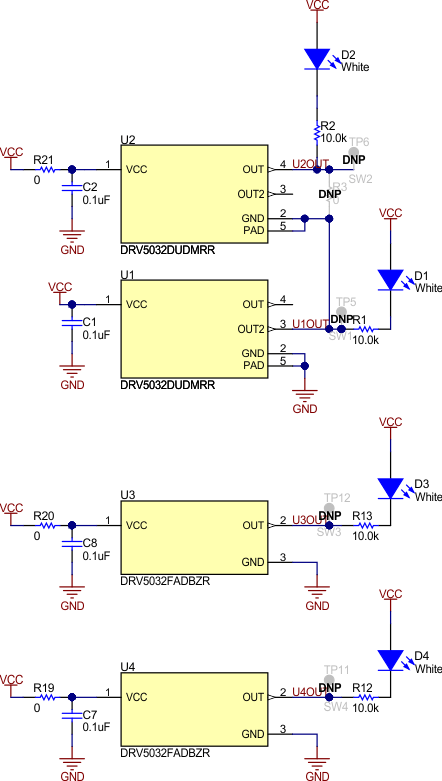
Figure 2-6 shows a snippet of the Hall-effect switch portion of the design, where the parts that are labeled U1, U2, U3, and U4 are the Hall-effect switches. In the design, U1 is the primary switch for waking the system up when the trigger is pressed, U2 is the stray field sensor, and U3 and U4 are the tamper Hall sensors.
 Figure 2-6 Schematic Snippet of Hall-Effect Switch Portion of Design
The DRV5032 is used for each of the four Hall-effect switches in the design. All four of these switches have a 20-Hz sampling rate, a push-pull output type, a test point on the board for probing the switch output, and an LED on the board for visually indicating the status of each switch. Table 2-2 shows how the configurations of the different Hall switches vary in this design.
| BOARD DESIGNATOR |
PURPOSE | DEVICE VERSION | THRESHOLD VALUES | MAGNETIC RESPONSE | PACKAGE | POWER STATE |
|---|---|---|---|---|---|---|
| U1 | Wake-up sensor | DRV5032DU | Output asserted low if B > 3.9 mT. Output asserted high if B <0.9 mT. | Unipolar: Responds to south (positive) pole of magnet (OUT2 pin of device is used) applied near top of package | X2SON | Always powered and enabled |
|
U2 |
Stray-field sensor | DRV5032DU | Output asserted low if B < -3.9 mT. Output asserted high if B > -0.9 mT. | Unipolar: Responds to north (negative) pole of magnet (OUT pin of device is used) applied near top of the package. | X2SON | Powered when resistor R21 populated and the OUT2 pin of U1 is asserted low |
|
U3 |
Tamper sensor 1 | DRV5032FA | Output asserted low if |B| > 4.8 mT. Output asserted high if |B| <0.5 mT. | Omnipolar: responds to north and south poles of magnet applied near top of package. | SOT-23 | Always powered if resistor R20 populated |
|
U4 |
Tamper sensor 2 | DRV5032FA | Output asserted low if |B| > 4.8 mT. Output asserted high if |B| <0.5 mT. | Omnipolar: responds to north and south poles of magnet applied near top of package. | SOT-23 | Always powered if resistor R19 populated |
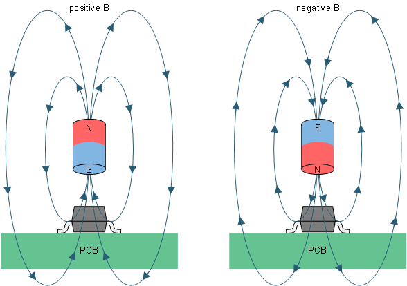
For the DRV5032, a negative field is defined as when the north pole of a magnet is applied near the top of the package containing the device, as shown in Figure 2-7. A negative field is also detected when the south pole of a magnet is applied underneath the bottom of the package that has the device. A positive field is defined as when the south pole of a magnet is applied near the top of the package or when the north pole of a magnet is applied underneath the bottom of the package containing the device.
 Figure 2-7 Flux Direction Polarity
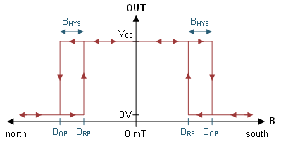
In the design, the 4-pin X2SON package of the DRV5032DU device variant is used for devices U1 and U2. This device variant is a dual output unipolar device, where each output only responds to either a positive field or a negative field. Figure 2-8 shows the output waveforms of the DRV5032DU device variant.
 Figure 2-8 DRV5032DU Output Waveforms
The OUT1 pin of the U1 and U2 devices (referred to as the OUT pin in Figure 2-7) only responds to negative magnetic flux density readings. This output is not affected by positive magnetic flux density readings. Figure 2-9 shows the data sheet spec for the BOP and BRP range of the OUT1 output . If the sensed magnetic flux density is less than the BOP spec of the OUT1 output of the DRV5032DU device variant, the OUT1 output will be asserted low. If the sensed magnetic flux density is greater than the BRP spec of the OUT1 output of the DRV5032DU device variant, the output will be asserted high. Based on the BOP,MIN and BRP,MAX range of the OUT1 Hall sensor, the OUT1 output is assured to be asserted low when the sensed magnetic flux density is less than -3.9 mT and asserted high when the sensed magnetic flux density is greater than -0.9 mT.
The OUT2 pin of the U1 and U2 devices, on the other hand, only responds to positive magnetic flux density readings. Figure 2-9 shows the data sheet spec for the BOP and BRP range of the OUT2 output. If the sensed magnetic flux density is greater than the BOP spec of the OUT2 output of the DRV5032DU device variant, the OUT2 output will be asserted low. If the sensed magnetic flux density is less than the BRP spec of the OUT2 output of the DRV5032DU device variant, the output will be asserted high. Based on the BOP,MIN and BRP,MAX range of the OUT2 Hall sensor, the OUT2 output is assured to be asserted low when the sensed magnetic flux density is greater than +3.9 mT and asserted high when the sensed magnetic flux density is less than +0.9 mT.
 Figure 2-9 BOP and BRP Range of DRV5032DU and DRV5032FA Outputs
For devices U3 and U4, the 3-pin SOT-23 package of the DRV5032FA device variant is used. This device is a single output omnipolar device, which responds to both positive and negative magnetic flux density readings the same way. Figure 2-10 shows the output waveform of the DRV5032FA device variant.
 Figure 2-10 DRV5032FA Output Waveform
The OUT pin of the U3 and U4 devices responds to both negative and positive magnetic flux density readings. Figure 2-8 shows the data sheet spec for the BOP and BRP range of this device variant. If the absolute value of the sensed magnetic flux density is greater than the BOP spec of the DRV5032FA, the OUT output will be asserted low. If the absolute value of the sensed magnetic flux density is less than the BRP spec of the DRV5032DU device variant, the output will be asserted high. Based on the BOP,MIN and BRP,MAX range of the Hall sensor, the OUT output is assured to be asserted low when the absolute value of the sensed magnetic flux density is greater than 4.8 mT and asserted high when the absolute value of the sensed magnetic flux density is less than 0.5 mT.