SWRU553A September 2019 – February 2020 AWR1243 , AWR2243
-
AWRx Cascaded Radar RF Evaluation Module (MMWCAS-RF-EVM)
- Trademarks
- 1 Getting Started
- 2 Hardware Description
- 3 Design Files and Software Tools
- 4 PCB Dimensions and Mounting Information
- 5 PCB Storage and Handling Recommendations
- 6 References
- 7 Regulatory Information
- Revision History
4 PCB Dimensions and Mounting Information
The field of view of the radar sensor is orthogonal to the PCB top layer where the etched antenna are placed. See the above antenna sections for more details on the antenna element gain patterns.
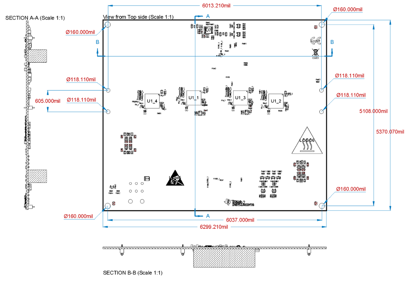
Mounting to the MMWCAS-DSP-EVM is accomplished through the 4, plated, through-holes in each corner of the PCB. An optional pattern of 4, plated through-hole are provided in the same lateral area as the AWRx devices and are meant to support a user-designed heat-sink plate across theAWRx packages.
 Figure 29. MMWCAS-RF-EVM Overall Mechanical Dimensions and Mounting Drill Dimensions
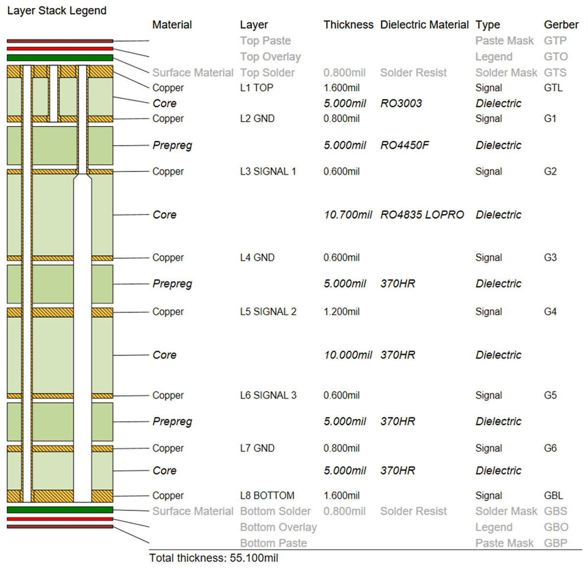
 The MMWCAS-RF-EVM PCB is composed of an 8-layer, heterogenous, sequential lamination, stack-up. Rogers RO3003 is used for the Layer 1 RF GCPW routing, etched antenna structtures and the 20 GHz LO splitters. RO4450F prepreg and RO4835 LoPro are used to create Stripline routing on Layer 3 for 20 GHz LO distribution. The lower 4 core and prepreg layers are in Isola 370HR. These layers are dedicated to power distribution and high-speed digital routing.
 Figure 30. MMWCAS-RF-EVM PCB and Drill Stack-Up Table
 Three via types are utilized throughout the design:
- L1-L8, 12.2mil drill, 22.4 mil pad - primary via used throughout the design for power and high-speed digital routing
- L1-L2, 5.9 mil drill, 13.77 mil pad (blind, micro-via) - L1 to L2 ground plane shorting for RF and LO routing distribution
- L1-L3, 12 mil drill, 24 mil pad, (backdrilled up to L3) - 20 GHz LO distribution L1 GCPW to L3 Stripline transition