SWRU553A September 2019 – February 2020
-
AWRx Cascaded Radar RF Evaluation Module (MMWCAS-RF-EVM)
- Trademarks
- 1 Getting Started
- 2 Hardware Description
- 3 Design Files and Software Tools
- 4 PCB Dimensions and Mounting Information
- 5 PCB Storage and Handling Recommendations
- 6 References
- 7 Regulatory Information
- Revision History
2.1 Block Diagram
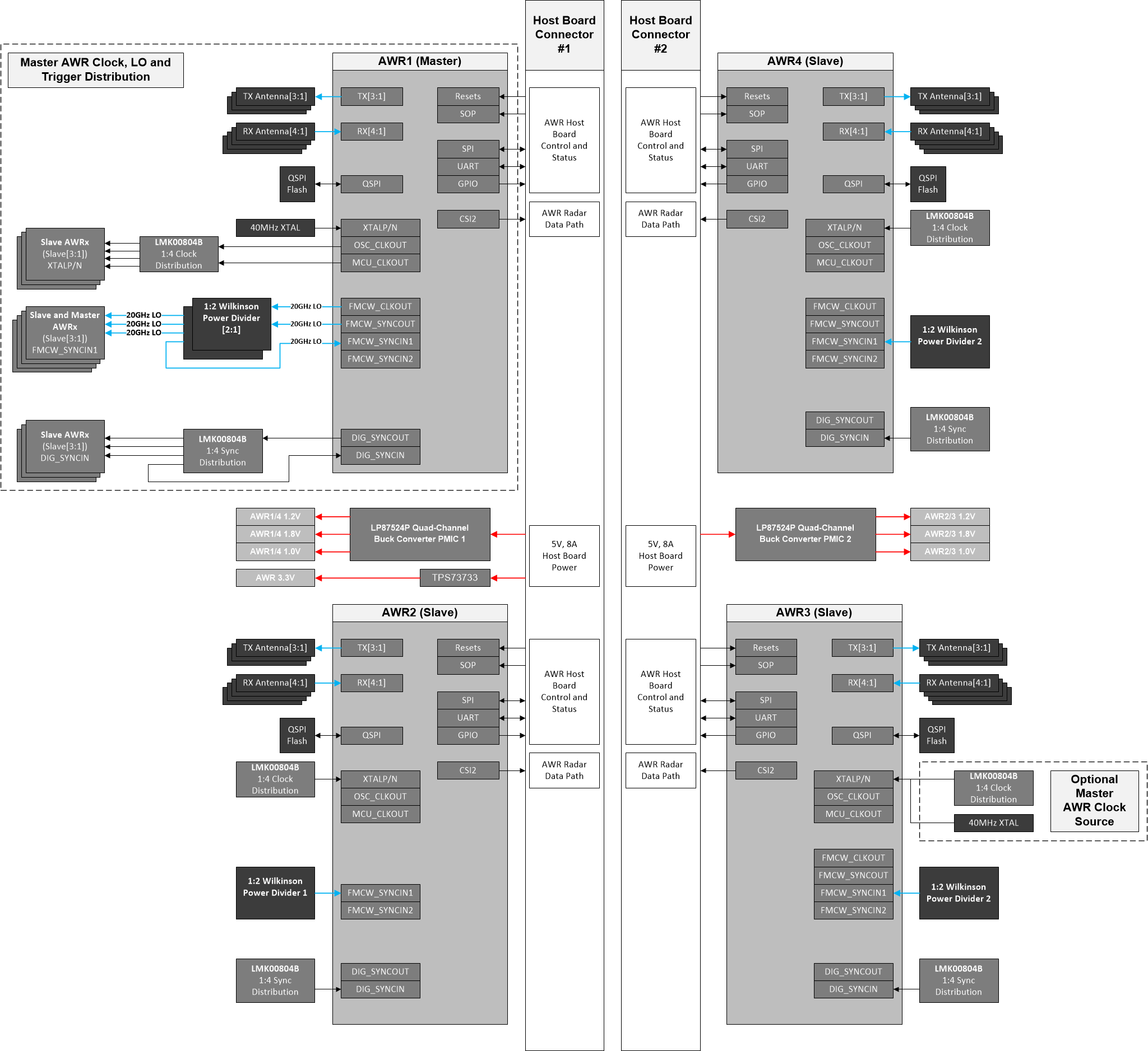
The MMWAVCAS-RF-EVM consists of four AWR mmWave SoC and their associated power, clocking, synchronization, LO and RF TX and RX circuits. Each AWRx RF TX and RX port is routed to an etched, series-fed, patch antenna element. Each AWRx on the RF board has a 4-port CSI2.0 transmitter which is used for sending radar IQ ADC data samples to an attached host processor CSI2.0 receiver set. All of the AWRx configuration, control and reset lines are made available on two host interface connectors (J4 and J5) implemented with Hirose FX23-120 connectors.
 Figure 4. MMWAVCAS-RF-EVM System Block Diagram
 The AWR devices are separated into Master and Slave classes of devices. AWRx #1, the Master device, utilizes the AWRx architecture built in VCO, LO distribution, clock distribution and frame synchronization distribution to provide 40 MHz clock, 20 GHz LO and frame synchronization to the other three Slave devices – AWRx #2, AWRx #3 and AWRx #4. This allows the system to generate and receive synchronous FMCW chirps across the four device AWRx array of transmitters and receivers.
The LO distribution follows the star-network configuration described in AWR2243 Cascade. The master AWRx feeds a network of two Wilkinson power dividers, which in turn provide synchronous LO for the Master and Slave PA and mixer subsystems. All clock distribution, synchronization distribution and LO distribution requirements are documented in this referenced application note.
The Cascade RF board accepts 5V DC, 8A (max) power primarily through the host board connectors J4 and J5. A separate 6-pin power connector (J6) is available as an alternate power path. The primary 5V system rail provided by the host board is converted into the variousAWRx device rails by the LP87524P quad-channel, monolithic, buck-converter.