SWRU553A September 2019 – February 2020
-
AWRx Cascaded Radar RF Evaluation Module (MMWCAS-RF-EVM)
- Trademarks
- 1 Getting Started
- 2 Hardware Description
- 3 Design Files and Software Tools
- 4 PCB Dimensions and Mounting Information
- 5 PCB Storage and Handling Recommendations
- 6 References
- 7 Regulatory Information
- Revision History
2 Hardware Description
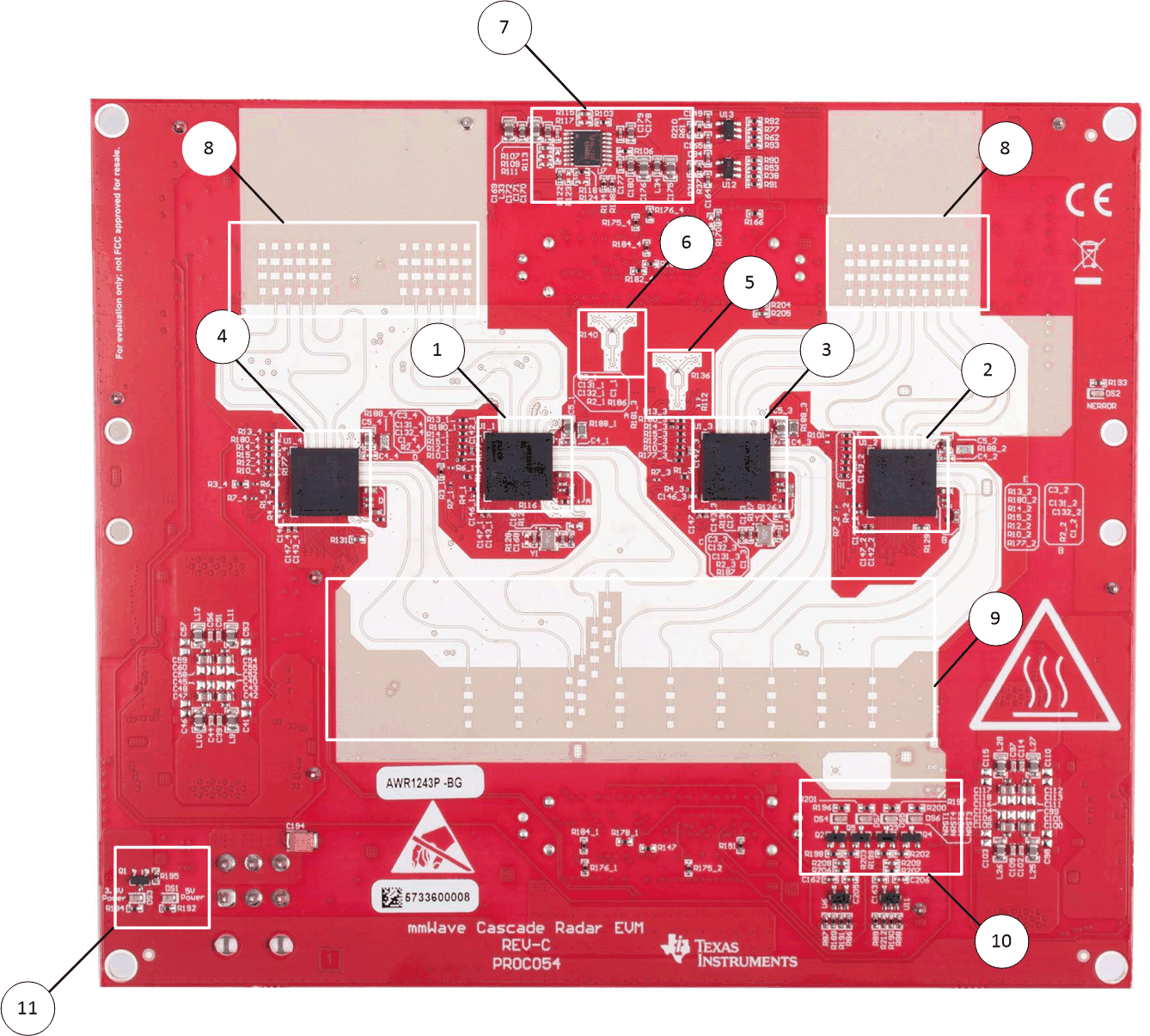
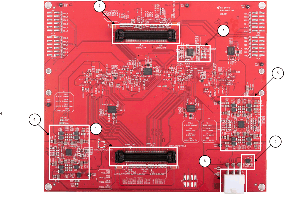
Figure 2 and Figure 3 show the front and rear views of the evaluation board, respectively. The front (top layer) of the board primarily includes the AWRx devices and the embedded antenna arrays and 20 GHz LO splitters. The back (bottom layer) of the board primarily includes the host board connectors, power supplies (PMIC), most other support IC and most passives.
 Figure 2. MMWAVCAS-RF-EVM Front View
 Front View Callouts:
- AWRx #1 “Master” (U1_1)
- AWRx #2 “Slave 1” (U1_2)
- AWRx #4 “Slave 3” (U1_4)
- AWRx #3 “Slave 2” (U1_3)
- 20 GHz LO Wilkinson Power Divider #1 (FMCW_CLKOUT) AWR #1 and AWR #2
- 20 GHz LO Wilkinson Power Divider #2 (FMCW_SYNCOUT) AWR #3 and AWR #4
- LMK00804B (U4) AWRx 40 MHz clock distribution buffer
- Receive antenna array
- Transmit antenna array
- AWRx reset LED indicators
- System 5.0 V and 3.3 V power status indicators
 Figure 3. MMWAVCAS-RF-EVM Back View
 Back View Callouts:
- Host Board Connector #1 (J4) 5.0 V power, interfaces for AWRx #1, AWRx #2
- Host Board Connector #2 (J5) 5.0 V power, interfacesAWRx #3, AWRx #4
- LP87524P PMIC #2 (U4) powersAWRx #2 and AWRx #3
- LP87524P PMIC #1 (U3) powersAWRx #1 and AWRx #4
- TPS73733 5.0V to 3.3 V LDO (U5) provides system 3.3 V power
- Bench 5.0 V power connector (J6)
- LMK00804B (U8) AWRx digital synchronization distribution buffer