SPRUIQ4 May 2019 TMS320F280021 , TMS320F280021-Q1 , TMS320F280023 , TMS320F280023-Q1 , TMS320F280023C , TMS320F280025 , TMS320F280025-Q1 , TMS320F280025C , TMS320F280025C-Q1 , TMS320F280040-Q1 , TMS320F280040C-Q1 , TMS320F280041 , TMS320F280041-Q1 , TMS320F280041C , TMS320F280041C-Q1 , TMS320F280045 , TMS320F280048-Q1 , TMS320F280048C-Q1 , TMS320F280049 , TMS320F280049-Q1 , TMS320F280049C , TMS320F280049C-Q1 , TMS320F28374D , TMS320F28374S , TMS320F28375D , TMS320F28375S , TMS320F28375S-Q1 , TMS320F28376D , TMS320F28376S , TMS320F28377D , TMS320F28377D-EP , TMS320F28377D-Q1 , TMS320F28377S , TMS320F28377S-Q1 , TMS320F28378D , TMS320F28378S , TMS320F28379D , TMS320F28379D-Q1 , TMS320F28379S
- Introduction
- 1Getting Familiar With the Kit
-
2Hardware Overview
- 2.1 IDDK Evaluation Board
- 2.2 Functional Blocks
- 2.3 Processor Section
- 2.4 Control Processor Slot – H1
- 2.5 Expansion Processor Slots
- 2.6 Position Encoder Suite
- 2.7 Current Sensor Suite
- 2.8 Power Supplies and GND Plane Configurations
- 2.9 Rectifier and Inverter
- 2.10 DACs
- 2.11 Power Stage Disable Circuits
- 3Hardware Resource Mapping
2.9.1 Rectifier Stage
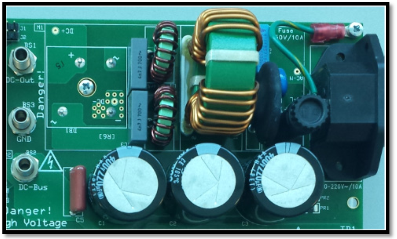
The rectifier is a block (M1). AC input to the board is fed through a 3-pronged connector (P1). The base of the board (which also acts as heat sink for power components) is connected to the EARTH pin through a pig-tail wire. A diode-bridge rectifier module is mounted on the bottom of the main printed-circuit-board (PCB).
 Figure 2-15 AC Line Input Filter and Rectifier
 NOTE
The fuse is mounted on fuse holder F1 located close to connector P1
BS1, BS2, and BS3 banana jacks provide flexibility and experimenting with high-voltage power sources. BS1 extends access to unfiltered rectified output of the AC mains. BS2 is tied to the positive terminal of DC-link caps while BS3 is tied to power ground PGND. Figure 2-16 shows how this configuration helps power the board with an external variable DC supply through BS2 and BS3, bypassing the rectifier. Figure 2-17 shows how BS1 and BS2 can connect through a banana cable before turning on the AC when appropriate to restore the AC supply to the board.