SPRUIQ4 May 2019 TMS320F280021 , TMS320F280021-Q1 , TMS320F280023 , TMS320F280023-Q1 , TMS320F280023C , TMS320F280025 , TMS320F280025-Q1 , TMS320F280025C , TMS320F280025C-Q1 , TMS320F280040-Q1 , TMS320F280040C-Q1 , TMS320F280041 , TMS320F280041-Q1 , TMS320F280041C , TMS320F280041C-Q1 , TMS320F280045 , TMS320F280048-Q1 , TMS320F280048C-Q1 , TMS320F280049 , TMS320F280049-Q1 , TMS320F280049C , TMS320F280049C-Q1 , TMS320F28374D , TMS320F28374S , TMS320F28375D , TMS320F28375S , TMS320F28375S-Q1 , TMS320F28376D , TMS320F28376S , TMS320F28377D , TMS320F28377D-EP , TMS320F28377D-Q1 , TMS320F28377S , TMS320F28377S-Q1 , TMS320F28378D , TMS320F28378S , TMS320F28379D , TMS320F28379D-Q1 , TMS320F28379S
- Introduction
- 1Getting Familiar With the Kit
-
2Hardware Overview
- 2.1 IDDK Evaluation Board
- 2.2 Functional Blocks
- 2.3 Processor Section
- 2.4 Control Processor Slot – H1
- 2.5 Expansion Processor Slots
- 2.6 Position Encoder Suite
- 2.7 Current Sensor Suite
- 2.8 Power Supplies and GND Plane Configurations
- 2.9 Rectifier and Inverter
- 2.10 DACs
- 2.11 Power Stage Disable Circuits
- 3Hardware Resource Mapping
2.8 Power Supplies and GND Plane Configurations
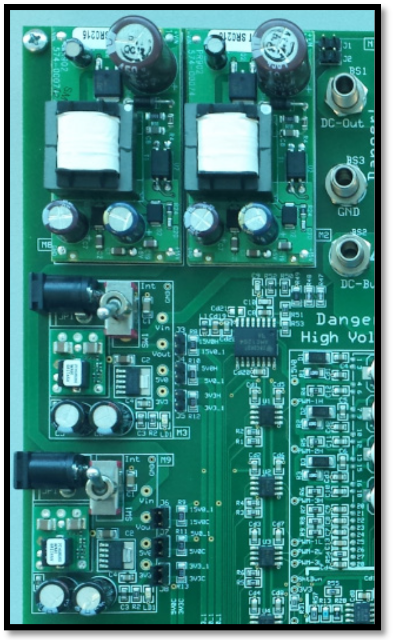
The kit has two identical onboard switching power-supply modules (M2 and M8) that take in DC-bus voltage though J1 and J2 jumpers, respectively. Each module delivers an isolated 15-V (400 mA rated) output to identical linear regulator blocks M3 and M9, respectively. The blocks deliver 5 V and 3.3 V to their local GNDs, respectively. M3 (M9) has a power-supply jack (JP1) and a toggle switch (SW1).
An external,15-V power supply can be fed in through JP1 while SW1 selects between the local 15 V from M2 (M8) and the external supply feeds the linear regulators of M3 (M9). TI prefers an external power supply to power the controller during code development so the board operates at low voltage. This low-voltage operation ensures safe operation without a high-voltage node on the board. Figure 2-11 shows the power supply block.
 Figure 2-11 Power Supply Block
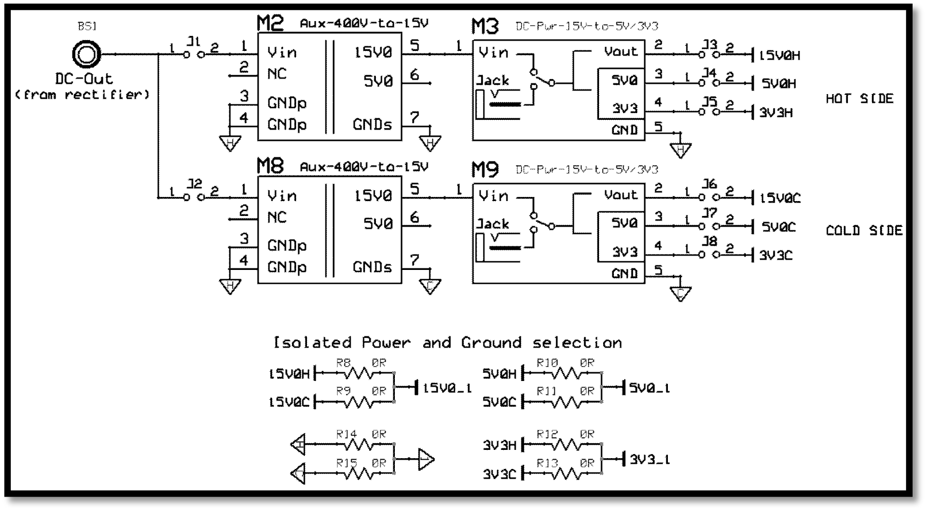
 M3 powers the gate-drive circuits of the inverter (the HOT side) while M9 powers the functional safety and real-time connectivity processors on the H7 and H8 connectors (the COLD side). The control CPU and its interface circuits can either connect to HOT side or COLD side, depending on a set of zero Ω resistor bridges (R8 through R13). You can use only M3 or M9 to power either side by suitably populating a set of jumpers (J3 through J8). Figure 2-12 shows the circuit diagram and Table 2-2 shows the possible configurations.
 Figure 2-12 Schematic Configuration of Power Supplies
 Table 2-2 Power Supply Connection Configuration
| Configuration Number | GND Plane Connection | HOT Side Parts | COLD Side Parts | ||||
| J3 to J5 | R8, R10, R12 | R14 | J6 to J8 | R9, R11, R13 | R15 | ||
| 1 | HOT -→ M3
COLD → M9 CONTROL → HOT |
√ | √ | √ | √ | X | X |
| 2 Default | HOT → M3
COLD → M9 CONTROL → COLD |
√ | X | X | √ | √ | √ |
| 3 | HOT → M3
COLD → M3 CONTROL → HOT |
√ | √ | √ | X | √ | √ |
| 4 | HOT → M9
COLD → M9 CONTROL → HOT |
X | √ | √ | √ | √ | √ |
The first and second line entries in Table 2-2 are cases that require separate HOT and COLD grounds, the control GND be tied to either HOT GND (as in line 1), or COLD GND (as in line 2). The default GND configuration of the kit out of the box is as in line 2.Line entries 3 and 4 have all GNDs tied together, which makes them all HOT and powered by either M3 or M9.
NOTE
If you choose the HOT control GND configuration, it enables direct measurement of phase voltages and currents through precision resistors. To use this feature, populate resistors R12, R31, R58, R59, and R47–R50 and capacitors C15-C18 (DNPs normally) in M4 (inverter) section of the board.
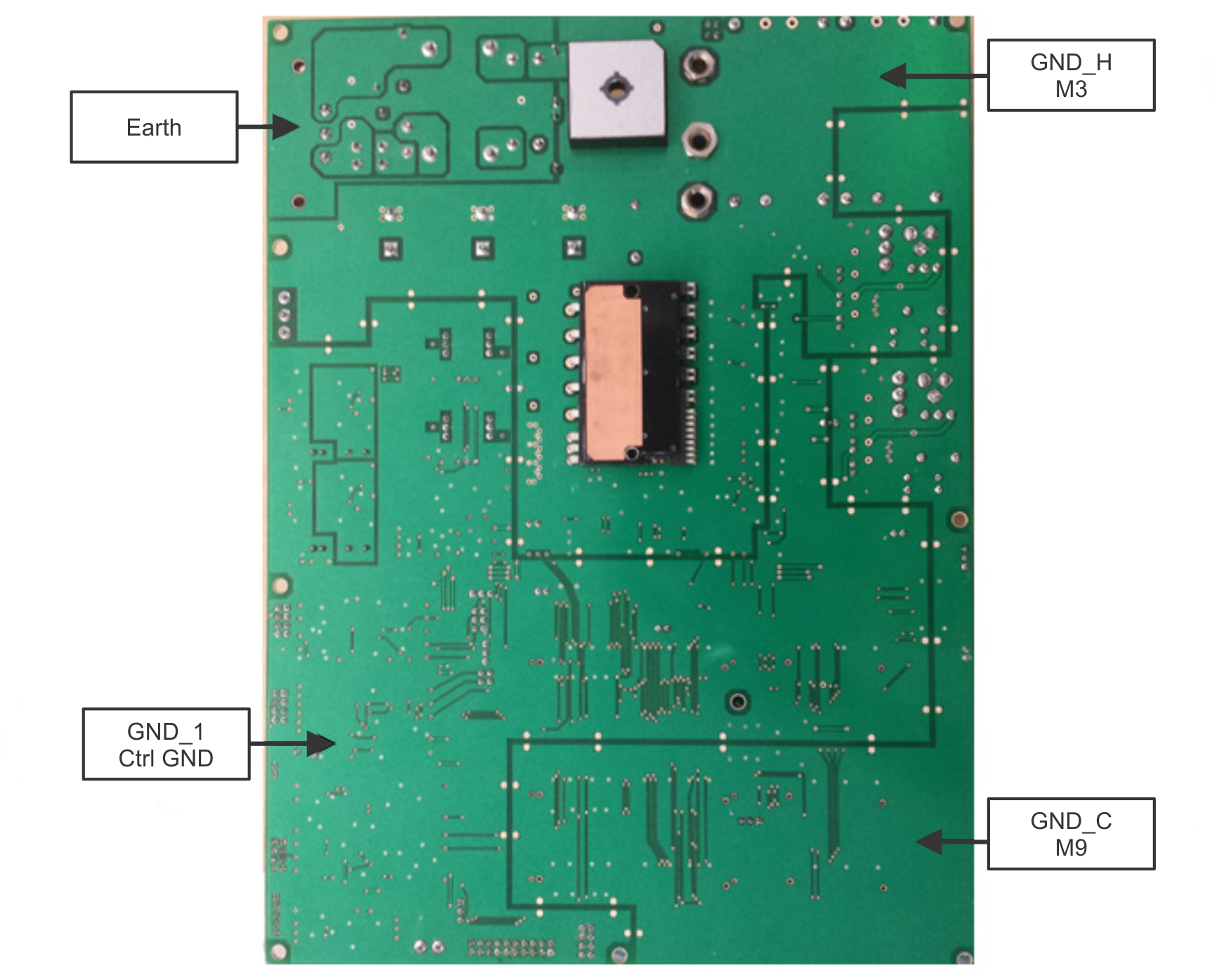
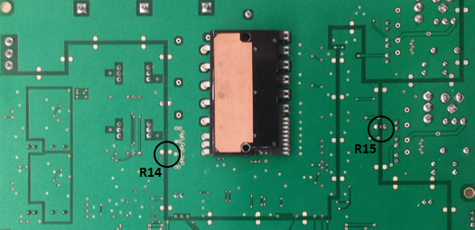
To power the board out of M9, populate J6 through J8 jumpers and R8 through R13 resistors in the main section of the board. Connecting different GND planes, resistors R14 and R15 are present on the bottom of the board and are unlabeled. Figure 2-13 shows multiple 1206 resistor pads across the various GND planes in multiple locations. TI intends to provide an option to evaluate the impact of the locations tying GND planes together. Carefully identify the GND planes of M9 and M3 before populating these resistors.
 Figure 2-13 Various GND Planes on the Bottom of Board
 GND_H and GND_C are tied to M3 and M9, respectively.
The default power supply configuration of the IDDK board is line entry 4 in Table 2-2. This configuration powers the entire board with M9. Figure 2-14 shows the default GND plane connection configuration.
 Figure 2-14 Default Connection of Various GND Planes