SPRUIQ4 May 2019 TMS320F280021 , TMS320F280021-Q1 , TMS320F280023 , TMS320F280023-Q1 , TMS320F280023C , TMS320F280025 , TMS320F280025-Q1 , TMS320F280025C , TMS320F280025C-Q1 , TMS320F280040-Q1 , TMS320F280040C-Q1 , TMS320F280041 , TMS320F280041-Q1 , TMS320F280041C , TMS320F280041C-Q1 , TMS320F280045 , TMS320F280048-Q1 , TMS320F280048C-Q1 , TMS320F280049 , TMS320F280049-Q1 , TMS320F280049C , TMS320F280049C-Q1 , TMS320F28374D , TMS320F28374S , TMS320F28375D , TMS320F28375S , TMS320F28375S-Q1 , TMS320F28376D , TMS320F28376S , TMS320F28377D , TMS320F28377D-EP , TMS320F28377D-Q1 , TMS320F28377S , TMS320F28377S-Q1 , TMS320F28378D , TMS320F28378S , TMS320F28379D , TMS320F28379D-Q1 , TMS320F28379S
- Introduction
- 1Getting Familiar With the Kit
-
2Hardware Overview
- 2.1 IDDK Evaluation Board
- 2.2 Functional Blocks
- 2.3 Processor Section
- 2.4 Control Processor Slot – H1
- 2.5 Expansion Processor Slots
- 2.6 Position Encoder Suite
- 2.7 Current Sensor Suite
- 2.8 Power Supplies and GND Plane Configurations
- 2.9 Rectifier and Inverter
- 2.10 DACs
- 2.11 Power Stage Disable Circuits
- 3Hardware Resource Mapping
2.9.2 Inverter Stage
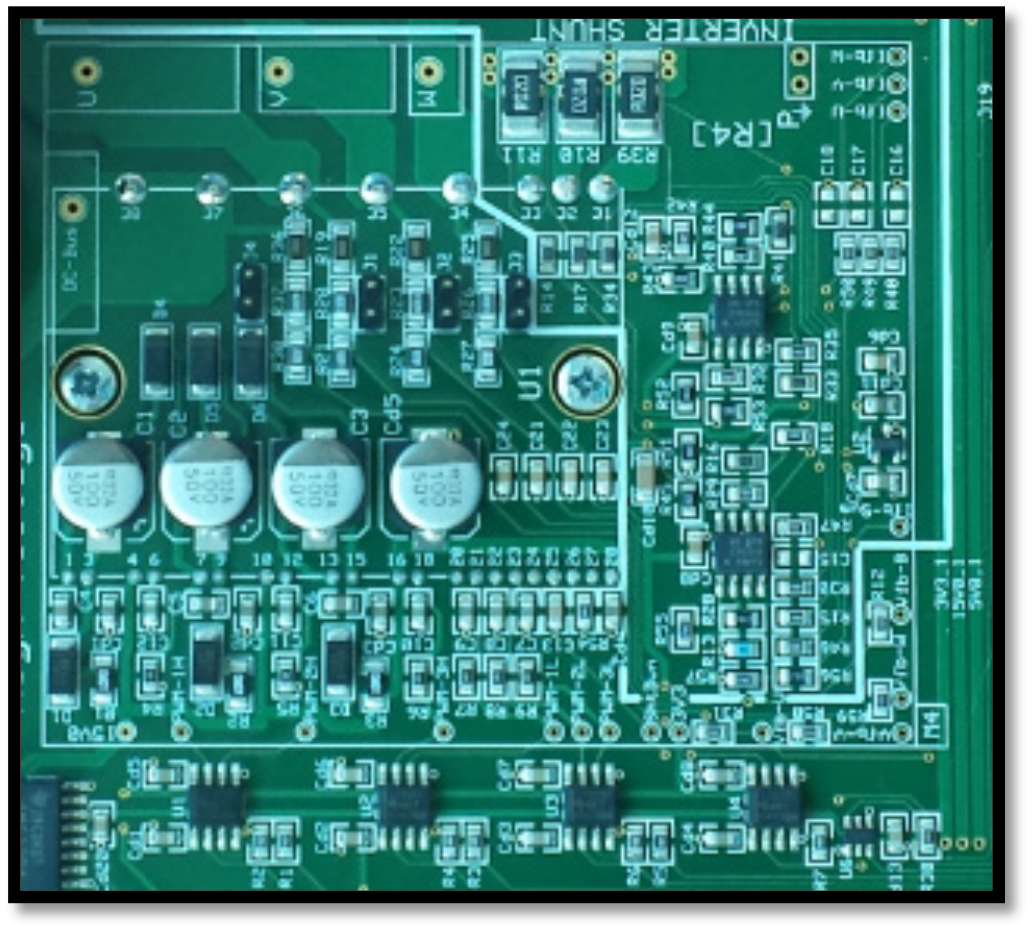
The inverter is a block (M4) with the gate drive circuits on top and IPM on the bottom. A large, thin aluminum base acts as the heat sink and base plate. The jumpers within this block (J1 through J4) are left open for sensing DC-bus voltages up to 400 V but can be populated to sense voltages less than 100 V. Figure 2-18 shows the 3-phase inverter.
 Figure 2-18 3-Phase Inverter
 WARNING
Removing heat sink will break the board connection to earth. Additional safety precautions may be needed to ensure safety of those handling the kit.