SPRACZ1 October 2021 F29H850TU , F29H859TU-Q1 , F29P329SM-Q1 , TMS320F280021 , TMS320F280021-Q1 , TMS320F280023 , TMS320F280023-Q1 , TMS320F280023C , TMS320F280025 , TMS320F280025-Q1 , TMS320F280025C , TMS320F280025C-Q1 , TMS320F280040-Q1 , TMS320F280040C-Q1 , TMS320F280041 , TMS320F280041-Q1 , TMS320F280041C , TMS320F280041C-Q1 , TMS320F280045 , TMS320F280048-Q1 , TMS320F280048C-Q1 , TMS320F280049 , TMS320F280049-Q1 , TMS320F280049C , TMS320F280049C-Q1 , TMS320F28044 , TMS320F28075 , TMS320F28075-Q1 , TMS320F28076 , TMS320F28374D , TMS320F28374S , TMS320F28375D , TMS320F28375S , TMS320F28375S-Q1 , TMS320F28376D , TMS320F28376S , TMS320F28377D , TMS320F28377D-EP , TMS320F28377D-Q1 , TMS320F28377S , TMS320F28377S-Q1 , TMS320F28378D , TMS320F28378S , TMS320F28379D , TMS320F28379D-Q1 , TMS320F28379S , TMS320F28384D , TMS320F28384D-Q1 , TMS320F28384S , TMS320F28384S-Q1 , TMS320F28386D , TMS320F28386D-Q1 , TMS320F28386S , TMS320F28386S-Q1 , TMS320F28388D , TMS320F28388S , TMS320F28P650DH , TMS320F28P650DK , TMS320F28P650SH , TMS320F28P650SK , TMS320F28P659DH-Q1 , TMS320F28P659DK-Q1 , TMS320F28P659SH-Q1
2.1 Expected Results Overview
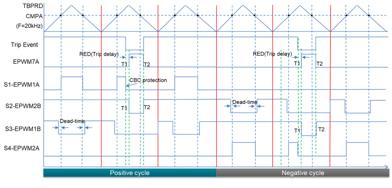
Figure 2-1 shows the expected EPWM protection results during positive and negative cycle operation conditions. In the given example, EPWM1A/2B/1B/2A are used for S1/2/3/4 control, respectively. And an extra EPWM output, EPWM7A in the example, is required to support the delayed protection logic. The trip signal is simulated and generated with an EPWM output, EPWM8A here, for the quick validation purpose.
Take the positive cycle operation as example, whenever the trip event occurs, EPWM1A and EPWM1B, which are configured with cycle-by-cycle tripping (CBC) action, are shut down immediately, while EPWM2B will be forced down after a Trip delay. Besides, when trip event disappears, EPWM2B will turn high immediately, which is also aligned with the basic recover requirement.
 Figure 2-1 Expected EPWM Protection
Results During Positive and Negative Cycle Operation Conditions
 Note that the given example code is based on F28004x, and it can be easily migrated to any other C2000 devices with Type 4 EPWM. And the code, built with the Driverlib API format, makes it more flexible to change or add the selected EPWM modules for different FET controls. Though the example is designed for single phase three-level inverters, the same configuration method can be used for three phase inverter topology, with six EPWM modules for main FETs control and one auxiliary EPWM channel needed. The example project discussed in this application report is available in the latest C2000WARE-DIGITALPOWER-SDK, navigating to the directory C:\ti\c2000\C2000Ware_DigitalPower_SDK_X_XX_XX_XX\libraries\3_level_inv_delayed_protection_scheme\examples.