SPRAC21A June 2016 – June 2019 OMAP-L132 , OMAP-L138 , TDA2E , TDA2EG-17 , TDA2HF , TDA2HG , TDA2HV , TDA2LF , TDA2P-ABZ , TDA2P-ACD , TDA2SA , TDA2SG , TDA2SX , TDA3LA , TDA3LX , TDA3MA , TDA3MD , TDA3MV
-
TDA2xx and TDA2ex Performance
- Trademarks
- 1 SoC Overview
- 2 Cortex-A15
- 3 System Enhanced Direct Memory Access (System EDMA)
- 4 DSP Subsystem EDMA
- 5 Embedded Vision Engine (EVE) Subsystem EDMA
- 6 DSP CPU
- 7 Cortex-M4 (IPU)
- 8 USB IP
- 9 PCIe IP
- 10 IVA-HD IP
- 11 MMC IP
- 12 SATA IP
- 13 GMAC IP
- 14 GPMC IP
- 15 QSPI IP
- 16 Standard Benchmarks
- 17
Error Checking and Correction (ECC)
- 17.1 OCMC ECC Programming
- 17.2 EMIF ECC Programming
- 17.3 EMIF ECC Programming to Starterware Code Mapping
- 17.4 Careabouts of Using EMIF ECC
- 17.5 Impact of ECC on Performance
- 18 DDR3 Interleaved vs Non-Interleaved
- 19 DDR3 vs DDR2 Performance
- 20 Boot Time Profile
- 21 L3 Statistics Collector Programming Model
- 22 Reference
- Revision History
3.2 System EDMA Observations
NOTE
On the TDA2xx and TDA2ex device, all transfer controllers yield identical performance for all transfer scenarios because both TCs have the same configuration, and most importantly the same FIFOSIZE for a given burst size.
EDMA channel parameters allow many different transfer configurations. Typical transfer configurations result in transfer controllers bursting the read write data in default burst size chunks, thereby, keeping the busses fully utilized. However, in some configurations, the TC issues less than optimally sized read and write commands (less than default burst size), reducing performance. To properly design a system, it is important to know which configurations offer the best performance for high-speed operations.
On TDA2xx and TDA2ex, there are two transfer controllers to move data between slave end points. The default configuration for the transfer controllers is shown in Table 13.
Table 13. Default Configuration for the Transfer Controllers
| Name | Description | TC0 | TC1 |
|---|---|---|---|
| TCCFG[2:0] FIFOSIZE | Channel FIFO Size | 1024 Bytes | 1024 Bytes |
| TCCFG[5:4] BUSWIDTH | Data Transfer Bus Width | 16 Bytes | 16 Bytes |
| TCCFG[9:8] DSTREGDEPTH | Destination Register Depth | 4 entries | 4 entries |
| DBS (Default Burst Size) | Size of each data burst | Configurable | Configurable |
The individual TC performance for paging and memory-to-memory transfers is essentially dictated by the TC configuration. In most scenarios, the FIFOSIZE and default burst size configuration for the TC have the most significant impact on the TC performance; the BUSWIDTH configuration is dependent on the device architecture and the DSTREGDEPTH values impact the number of in-flight transfers.
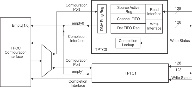
 Figure 11. EDMA Third-party Transfer Controller (EDMA_TPTC) Block Diagram
 The default burst size (DBS) can be controlled with the CTRL_CORE_CONTROL_IO_1 register in the TDA2xx and TDA2ex Control Module Registers, as shown in Table 14.
Table 14. CTRL_CORE_CONTROL_IO_1
| Address offset | 0x0000 0554 | ||||
| Physical Address | 0x4A00 2554 | Instance | CTRL_MODULE_CORE | ||
| Description | Register to configure some IP level signals | ||||
| Type | RW | ||||
| 31 | 30 | 29 | 28 | 27 | 26 | 25 | 24 | 23 | 22 | 21 | 20 | 19 | 18 | 17 | 16 | 15 | 14 | 13 | 12 | 11 | 10 | 9 | 8 | 7 | 6 | 5 | 4 | 3 | 2 | 1 | 0 |
| RESERVED | MMU2_DISABLE | RESERVED | MMU1_DISABLE | RESERVED | TC1_DEFAULT_BURST_SIZE | RESERVED | TC0_DEFAULT_BURST_SIZE | RESERVED | GMII2_SEL | RESERVED | GMII1_SEL | ||||||||||||||||||||
| Bits | Field Name | Description | Type | Reset |
|---|---|---|---|---|
| 31:21 | RESERVED | Reserved | R | 0x0 |
| 20 | MMU2_DISABLE |
MMU2 DISABLE setting |
RW | 0x0 |
| 19:17 | RESERVED |
Reserved |
R | 0x0 |
| 16 | MMU1_DISABLE |
MMU1 DISABLE setting |
RW | 0x0 |
| 15:14 | RESERVED |
Reserved |
R | 0x0 |
| 13:12 | TC1_DEFAULT_BURST_SIZE |
EDMA TC1 DEFAULT BURST SIZE setting |
RW | 0x3 |
| 11:10 | RESERVED |
Reserved |
R | 0x0 |
| 9:8 | TC0_DEFAULT_BURST_SIZE |
EDMA TC0 DEFAULT BURST SIZE setting |
RW | 0x3 |
| 7:6 | RESERVED |
Reserved |
R | 0x0 |
| 5:4 | GMII2_SEL |
GMII2 selection setting |
RW | 0x0 |
| 3:2 | RESERVED |
Reserved |
R | 0x0 |
| 1:0 | GMII1_SEL |
GMII1 selection setting |
RW | 0x0 |
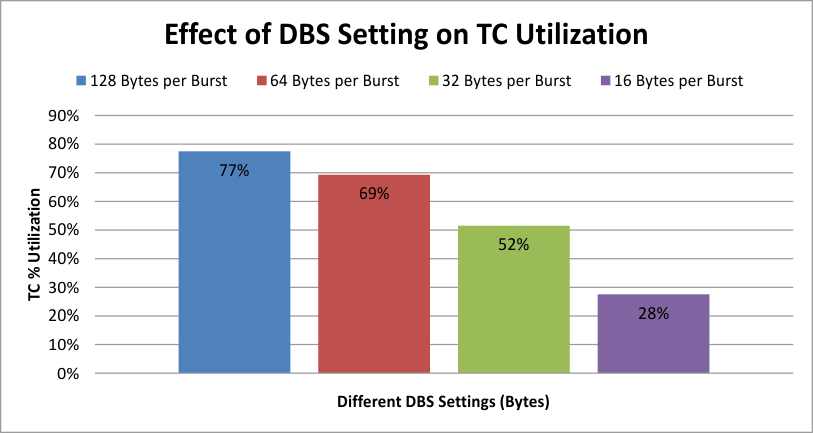
The effect of the DBS setting on the TC% utilization can be realized with the graph in Figure 12. The data transfer used to obtain these results is a DDR-to-DDR transfer of 16 MB. It is observed that the default setting of 128 bytes per burst generates the maximum TC utilization.
 Figure 12. Effect of DBS on System EDMA TC Utilization
 The TC read and write controllers in conjunction with the source and destination register sets are responsible for issuing optimally-sized reads and writes to the slave endpoints. An optimally-sized command is defined by the transfer controller default burst size (DBS).
The EDMA_TPTC attempts to issue the largest possible command size as limited by the DBS value or the ABCNT_n[15:0] ACNT and ABCNT_n[31:16] BCNT value of the TR. The EDMA_TPTC obeys the following rules:
- The read and write controllers always issue commands less than or equal to the DBS value.
- The first command of a 1D transfer command always aligns the address of subsequent commands to the DBS value.
Table 15 lists the TR segmentation rules that are followed by the EDMA_TPTC. In summary, if the ABCNT_n[15:0] ACNT value is larger than the DBS value, then the EDMA_TPTC breaks the ABCNT_n[15:0] ACNT array into DBS-sized commands to the source and destination addresses. Each ABCNT_n[31:16] BCNT number of arrays are then serviced in succession.
For BCNT arrays of ACNT bytes (that is, a 2D transfer), if the ABCNT_n[15:0] ACNT value is less than or equal to the DBS value, then the TR may be optimized into a 1D-transfer in order to maximize efficiency. The optimization takes place if the EDMA_TPTC recognizes that the 2D-transfer is organized as a single dimension (ABCNT_n[15:0] ACNT == BIDX_n) and the ACNT value is a power of 2.
Table 15. System EDMA TC Optimization Rules
| ACNT ≤ DBS | ACNT is Power of 2 | BIDX = ACNT | BCNT ≤ 1023 | SAM/DAM = Increment | Description |
|---|---|---|---|---|---|
| Yes | Yes | Yes | Yes | Yes | Optimized |
| No | X | X | X | X | Not Optimized |
| X | No | X | X | X | Not Optimized |
| X | X | No | X | X | Not Optimized |
| X | X | X | No | X | Not Optimized |
| X | X | X | X | No | Not Optimized |
In summary, Table 16 lists the factors that affect the EDMA performance.
Table 16. Factors Affecting System EDMA Performance
| Factors | Impact | General Recommendation |
|---|---|---|
| Source/Destination Memory | The transfer speed depends on SRC/DST memory bandwidth. | Know the nature of the source and destination memory, specifically the frequency of operation and the bus width. |
| Transfer Size | Throughput is less for small transfers due to transfer overhead and latency. | Configure EDMA for larger transfer size as throughput, small transfer size is dominated by transfer overhead. |
| A-Sync/AB-Sync | Performance depends on the number of TRs (Transfer Requests). More TRs would mean more overhead. | Using AB-Sync transfers gives better performance than chaining A-Sync transfers. |
| Source/Destination Bidx | Optimization will not be done if BIDX is not equal to ACNT value optimization guidelines. | Whenever possible, follow the EDMA TC optimization guidelines. See the TPTC spec for optimization details. |
| Queue TC Usage | Performance is the same for both TCs. | Both TCs have the same configuration and show the same performance. |
| Burst Size | Decides the largest possible read/write command submission by TC. | The default burst size for all transfer controllers is 128 bytes. This also results in most efficient transfers/throughput in most memory-to-memory transfer scenarios. |
| Source/Destination Alignment | Slight performance degradation if source/destination are not aligned to Default Burst Size (DBS) boundaries. | For smaller transfers, as much as possible, source and destination addresses should be aligned across DBS boundaries. |