SPRAC21A June   2016  – June 2019 OMAP-L132 , OMAP-L138 , TDA2E , TDA2EG-17 , TDA2HF , TDA2HG , TDA2HV , TDA2LF , TDA2P-ABZ , TDA2P-ACD , TDA2SA , TDA2SG , TDA2SX , TDA3LA , TDA3LX , TDA3MA , TDA3MD , TDA3MV


  1.   TDA2xx and TDA2ex Performance
    1.     Trademarks
    2. SoC Overview
      1. 1.1 Introduction
      2. 1.2 Acronyms and Definitions
      3. 1.3 TDA2xx and TDA2ex System Interconnect
      4. 1.4 Traffic Regulation Within the Interconnect
        1. 1.4.1 Bandwidth Regulators
        2. 1.4.2 Bandwidth Limiters
        3. 1.4.3 Initiator Priority
      5. 1.5 TDA2xx and TDA2ex Memory Subsystem
        1. 1.5.1 Controller/PHY Timing Parameters
        2. 1.5.2 Class of Service
        3. 1.5.3 Prioritization Between DMM/SYS PORT or MPU Port to EMIF
      6. 1.6 TDA2xx and TDA2ex Measurement Operating Frequencies
      7. 1.7 System Instrumentation and Measurement Methodology
        1. 1.7.1 GP Timers
        2. 1.7.2 L3 Statistic Collectors
    3. Cortex-A15
      1. 2.1 Level1 and Level2 Cache
      2. 2.2 MMU
      3. 2.3 Performance Control Mechanisms
        1. 2.3.1 Cortex-A15 Knobs
        2. 2.3.2 MMU Page Table Knobs
      4. 2.4 Cortex-A15 CPU Read and Write Performance
        1. 2.4.1 Cortex-A15 Functions
        2. 2.4.2 Setup Limitations
        3. 2.4.3 System Performance
          1. 2.4.3.1 Cortex-A15 Stand-Alone Memory Read, Write, Copy
          2. 2.4.3.2 Results
    4. System Enhanced Direct Memory Access (System EDMA)
      1. 3.1 System EDMA Performance
        1. 3.1.1 System EDMA Read and Write
        2. 3.1.2 System EDMA Results
      2. 3.2 System EDMA Observations
    5. DSP Subsystem EDMA
      1. 4.1 DSP Subsystem EDMA Performance
        1. 4.1.1 DSP Subsystem EDMA Read and Write
        2. 4.1.2 DSP Subsystem EDMA Results
      2. 4.2 DSP Subsystem EDMA Observations
    6. Embedded Vision Engine (EVE) Subsystem EDMA
      1. 5.1 EVE EDMA Performance
        1. 5.1.1 EVE EDMA Read and Write
        2. 5.1.2 EVE EDMA Results
      2. 5.2 EVE EDMA Observations
    7. DSP CPU
      1. 6.1 DSP CPU Performance
        1. 6.1.1 DSP CPU Read and Write
        2. 6.1.2 Code Setup
          1. 6.1.2.1 Pipeline Copy
          2. 6.1.2.2 Pipeline Read
          3. 6.1.2.3 Pipeline Write
          4. 6.1.2.4 L2 Stride-Jmp Copy
          5. 6.1.2.5 L2 Stride-Jmp Read
          6. 6.1.2.6 L2 Stride-Jmp Write
      2. 6.2 DSP CPU Observations
      3. 6.3 Summary
    8. Cortex-M4 (IPU)
      1. 7.1 Cortex-M4 CPU Performance
        1. 7.1.1 Cortex-M4 CPU Read and Write
        2. 7.1.2 Code Setup
        3. 7.1.3 Cortex-M4 Functions
        4. 7.1.4 Setup Limitations
      2. 7.2 Cortex-M4 CPU Observations
        1. 7.2.1 Cache Disable
        2. 7.2.2 Cache Enable
      3. 7.3 Summary
    9. USB IP
      1. 8.1 Overview
      2. 8.2 USB IP Performance
        1. 8.2.1 Test Setup
        2. 8.2.2 Results and Observations
        3. 8.2.3 Summary
    10. PCIe IP
      1. 9.1 Overview
      2. 9.2 PCIe IP Performance
        1. 9.2.1 Test Setup
        2. 9.2.2 Results and Observations
    11. 10 IVA-HD IP
      1. 10.1 Overview
      2. 10.2 H.264 Decoder
        1. 10.2.1 Description
        2. 10.2.2 Test Setup
        3. 10.2.3 Test Results
      3. 10.3 MJPEG Decoder
        1. 10.3.1 Description
        2. 10.3.2 Test Setup
        3. 10.3.3 Test Results
    12. 11 MMC IP
      1. 11.1 MMC Read and Write Performance
        1. 11.1.1 Test Description
        2. 11.1.2 Test Results
      2. 11.2 Summary
    13. 12 SATA IP
      1. 12.1 SATA Read and Write Performance
        1. 12.1.1 Test Setup
        2. 12.1.2 Observations
          1. 12.1.2.1 RAW Performance
          2. 12.1.2.2 SDK Performance
      2. 12.2 Summary
    14. 13 GMAC IP
      1. 13.1 GMAC Receive/Transmit Performance
        1. 13.1.1 Test Setup
        2. 13.1.2 Test Description
          1. 13.1.2.1 CPPI Buffer Descriptors
        3. 13.1.3 Test Results
          1. 13.1.3.1 Receive/Transmit Mode (see )
          2. 13.1.3.2 Receive Only Mode (see )
          3. 13.1.3.3 Transmit Only Mode (see )
      2. 13.2 Summary
    15. 14 GPMC IP
      1. 14.1 GPMC Read and Write Performance
        1. 14.1.1 Test Setup
          1. 14.1.1.1 NAND Flash
          2. 14.1.1.2 NOR Flash
        2. 14.1.2 Test Description
          1. 14.1.2.1 Asynchronous NAND Flash Read/Write Using CPU Prefetch Mode
          2. 14.1.2.2 Asynchronous NOR Flash Single Read
          3. 14.1.2.3 Asynchronous NOR Flash Page Read
          4. 14.1.2.4 Asynchronous NOR Flash Single Write
        3. 14.1.3 Test Results
      2. 14.2 Summary
    16. 15 QSPI IP
      1. 15.1 QSPI Read and Write Performance
        1. 15.1.1 Test Setup
        2. 15.1.2 Test Results
        3. 15.1.3 Analysis
          1. 15.1.3.1 Theoretical Calculations
          2. 15.1.3.2 % Efficiency
      2. 15.2 QSPI XIP Code Execution Performance
      3. 15.3 Summary
    17. 16 Standard Benchmarks
      1. 16.1 Dhrystone
        1. 16.1.1 Cortex-A15 Tests and Results
        2. 16.1.2 Cortex-M4 Tests and Results
      2. 16.2 LMbench
        1. 16.2.1 LMbench Bandwidth
          1. 16.2.1.1 TDA2xx and TDA2ex Cortex-A15 LMbench Bandwidth Results
          2. 16.2.1.2 TDA2xx and TDA2ex Cortex-M4 LMBench Bandwidth Results
          3. 16.2.1.3 Analysis
        2. 16.2.2 LMbench Latency
          1. 16.2.2.1 TDA2xx and TDA2ex Cortex-A15 LMbench Latency Results
          2. 16.2.2.2 TDA2xx and TDA2ex Cortex-M4 LMbench Latency Results
          3. 16.2.2.3 Analysis
      3. 16.3 STREAM
        1. 16.3.1 TDA2xx and TDA2ex Cortex-A15 STREAM Benchmark Results
        2. 16.3.2 TDA2xx and TDA2ex Cortex-M4 STREAM Benchmark Results
    18. 17 Error Checking and Correction (ECC)
      1. 17.1 OCMC ECC Programming
      2. 17.2 EMIF ECC Programming
      3. 17.3 EMIF ECC Programming to Starterware Code Mapping
      4. 17.4 Careabouts of Using EMIF ECC
        1. 17.4.1 Restrictions Due to Non-Availability of Read Modify Write ECC Support in EMIF
          1. 17.4.1.1 Un-Cached CPU Access of EMIF
          2. 17.4.1.2 Cached CPU Access of EMIF
          3. 17.4.1.3 Non CPU Access of EMIF Memory
          4. 17.4.1.4 Debugger Access of EMIF via the Memory Browser/Watch Window
          5. 17.4.1.5 Software Breakpoints While Debugging
        2. 17.4.2 Compiler Optimization
        3. 17.4.3 Restrictions Due to i882 Errata
        4. 17.4.4 How to Find Who Caused the Unaligned Quanta Writes After the Interrupt
      5. 17.5 Impact of ECC on Performance
    19. 18 DDR3 Interleaved vs Non-Interleaved
      1. 18.1 Interleaved versus Non-Interleaved Setup
      2. 18.2 Impact of Interleaved vs Non-Interleaved DDR3 for a Single Initiator
      3. 18.3 Impact of Interleaved vs Non-Interleaved DDR3 for Multiple Initiators
    20. 19 DDR3 vs DDR2 Performance
      1. 19.1 Impact of DDR2 vs DDR3 for a Single Initiator
      2. 19.2 Impact of DDR2 vs DDR3 for Multiple Initiators
    21. 20 Boot Time Profile
      1. 20.1 ROM Boot Time Profile
      2. 20.2 System Boot Time Profile
    22. 21 L3 Statistics Collector Programming Model
    23. 22 Reference
  2.   Revision History

Asynchronous NOR Flash Single Read

Address access time (tACC) is equal to the delay from stable addresses to valid output data The chip enable access time (tCE) is the delay from stable CE# to valid data at the outputs. In order for the read data to be driven on to the data outputs, the OE# signal must be low for at least the output enable time (tOE) before valid data is available.

Figure 34 shows the read operation timing diagram at the Flash.
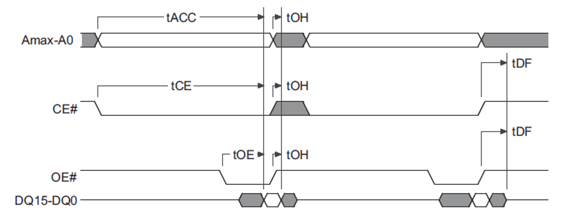
back_to_back_read_tacc_operation_timing_sprac21.pngFigure 34. Back-to-Back Read (tACC) Operation Timing Diagram

Figure 35 shows the read operation timing diagram with GPMC signal parameters.
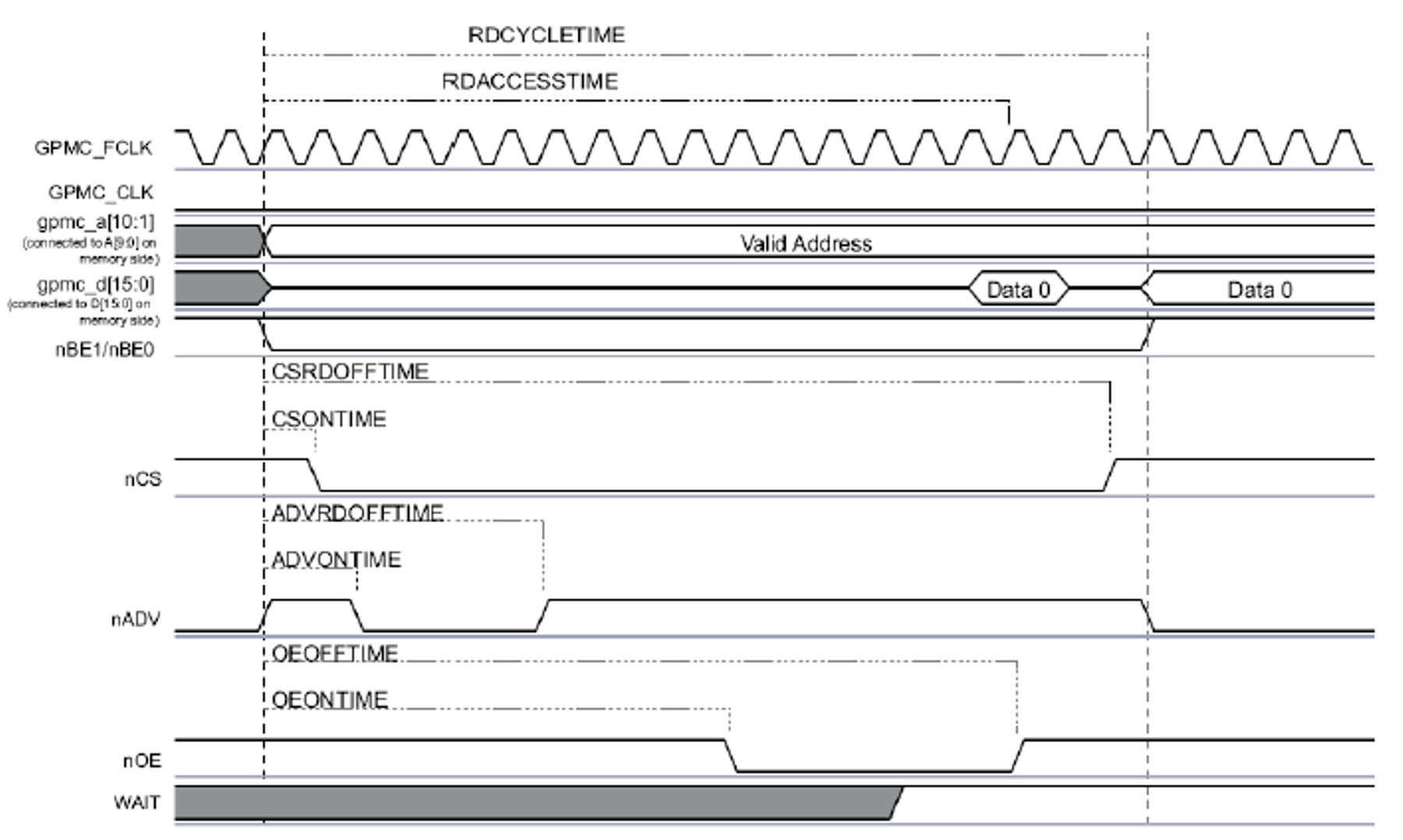
asynchronous_single_read_timing_parameters_sprac21.pngFigure 35. Asynchronous Single Read Timing Parameters

For the successful read operation to occur, GPMC timing parameters have to be set satisfying the Flash level timing values. Table 53 shows the optimum configuration for GPMC timing values for successful read operation. 1 GPMC clock =~ 3.7 ns. Here “Timeparagranularity” is set as 0x1, which will multiply the configured timing values by 2.

Table 53. Optimum Configuration for GPMC for Reads of NOR Flash Single Read

Signal Parameter Description Value Programmed
Read op RDACCESSTIME Address latch + Initial access time = 0ns + 110ns =
30 GPMC clock cycles
0x0F
RDCYCLETIME RDACCESSTIME + Data holding + tDF = 30 + 4 + 4 =
38 GPMC clock cycles
0x13
nCS CSONTIME Assert after address latch 0x00
CSRDOFFTIME RDACCESSTIME + Data holding = 30 + 4 = 34 GPMC clock cycles 0x11
nADV ADVONTIME Immediate assert with read cycle 0x00
ADVOFFTIME Provide ADV assertion duration of 2 cycles 0x01
nOE OEONTIME Assert after address latch 0x00
OEOFFTIME RDACCESSTIME + Dataholding 0x11