SNVA559C September 2012 – February 2019 LM2574 , LM2575-N , LM2575HV , LM2576 , LM2576HV , LM2577
-
Switching regulator fundamentals
- Trademarks
- 1 Switching Fundamentals
- 2 Switching Converter Topologies
- 3 Application Hints for Switching Regulators
- 4 Application Circuits
- 5 References and Related Products
- Revision History
2.8 Push-Pull Converter
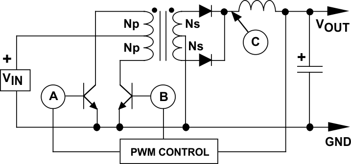
The Push-Pull converter uses two to transistors perform DC/DC conversion (see Figure 11).
 Figure 11. Push-Pull Converter
 The converter operates by turning on each transistor on alternate cycles (the two transistors are never on at the same time). Transformer secondary current flows at the same time as primary current (when either of the switches is on).
For example, when transistor A is turned on, the input voltage is forced across the upper primary winding with dot-negative polarity. On the secondary side, a dot-negative voltage will appear across the winding which turns on the bottom diode. This allows current to flow into the inductor to supply both the output capacitor and the load.
When transistor B is on, the input voltage is forced across the lower primary winding with dot-positive polarity. The same voltage polarity on the secondary turns on the top diode, and current flows into the output capacitor and the load.
An important characteristic of a Push-Pull converter is that the switch transistors have to be able the stand off more than twice the input voltage: when one transistor is on (and the input voltage is forced across one primary winding) the same magnitude voltage is induced across the other primary winding, but it is floating on top of the input voltage. This puts the collector of the turned-off transistor at twice the input voltage with respect to ground.
The double input voltage rating requirement of the switch transistors means the Push-Pull converter is best suited for lower input voltage applications. It has been widely used in converters operating in 12-V and 24-V battery-powered systems.
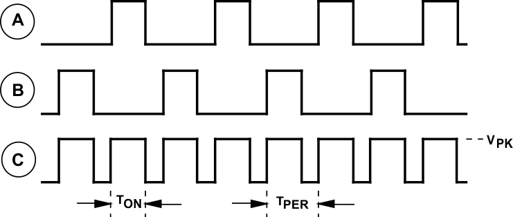
 Figure 12. Timing Diagram for Push-Pull Converter
 Figure 12 shows a timing diagram which details the relationship of the input and output pulses.
It is important to note that frequency of the secondary side voltage pulses is twice the frequency of operation of the PWM controller driving the two transistors. For example, if the PWM control chip was set up to operate at 50 kHz on the primary side, the frequency of the secondary pulses would be 100 kHz.
The DC output voltage is given by Equation 2:
The peak amplitude of the secondary pulses (VPK) is given by Equation 3:
This highlights why the Push-Pull converter is well-suited for low voltage converters. The voltage forced across each primary winding (which provides the power for conversion) is the full input voltage minus only the saturation voltage of the switch.
If MOSFET power switches are used, the voltage drop across the switches can be made extremely small, resulting in very high utilization of the available input voltage.
Another advantage of the Push-Pull converter is that it can also generate multiple output voltages (by adding more secondary windings), some of which may be negative in polarity. This allows a power supply operated from a single battery to provide all of the voltages necessary for system operation.
A disadvantage of Push-Pull converters is that they require very good matching of the switch transistors to prevent unequal ON times, because this will result in saturation of the transformer core (and failure of the converter).