SNVA559C September 2012 – February 2019 LM2574 , LM2575-N , LM2575HV , LM2576 , LM2576HV , LM2577
-
Switching regulator fundamentals
- Trademarks
- 1 Switching Fundamentals
- 2 Switching Converter Topologies
- 3 Application Hints for Switching Regulators
- 4 Application Circuits
- 5 References and Related Products
- Revision History
2.5 Buck-Boost (Inverting) Regulator
The Buck-Boost or Inverting regulator takes a DC input voltage and produces a DC output voltage that is opposite in polarity to the input. The negative output voltage can be either larger or smaller in magnitude than the input voltage.
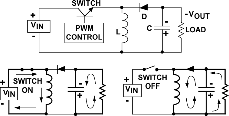
The Inverting regulator is shown in Figure 8.
 Figure 8. Buck-Boost (Inverting) Regulator
 When the switch is on, the input voltage is forced across the inductor, causing an increasing current flow through it. During the ON time, the discharge of the output capacitor is the only source of load current.
This requires that the charge lost from the output capacitor during the on time be replenished during the OFF time.
When the switch turns off, the decreasing current flow in the inductor causes the voltage at the diode end to swing negative. This action turns on the diode, allowing the current in the inductor to supply both the output capacitor and the load.
As shown, the load current is supplied by inductor when the switch is off, and by the output capacitor when the switch is on.