SNVA559C September 2012 – February 2019 LM2574 , LM2575-N , LM2575HV , LM2576 , LM2576HV , LM2577
-
Switching regulator fundamentals
- Trademarks
- 1 Switching Fundamentals
- 2 Switching Converter Topologies
- 3 Application Hints for Switching Regulators
- 4 Application Circuits
- 5 References and Related Products
- Revision History
4.5 Low Dropout, High Efficiency 5-V/3-A Buck Regulator
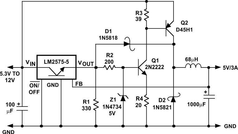
A circuit was developed which provides a 5-V/3-A regulated output voltage with very high efficiency and very low dropout voltage (see Figure 31). The customer required that the circuit be able to operate with an input voltage range of 6 V to 12 V, allowing only 1 V of dropout at the lowest input voltage.
 Figure 31. Low-Dropout 5-V/3-A regulator
 An unusual feature of this circuit is that it can stay in regulation with only 300 mV across the regulator. Also, the efficiency is highest (89%) at the lowest input voltage (buck converters are typically more efficient at higher input voltages).
The low (< 300 mV) dropout voltage is achieved by using an external PNP power transistor (Q2) as the main switching transistor (the other transistors in the circuit are drivers for Q2). With components values shown, Q2 has a saturation voltage of 200 mV at 3 A, which allows the 300 mV input-output differential requirement for the regulator to be met.
The switch inside the LM2575 drives the base of Q1 through R2. Note that the maximum collector current of Q1 (and the maximum base drive available for Q2) is limited by Z1 and R4. When Z1 clamps at 5V, the maximum current through Q1 is:
The maximum Q1 current (215 mA) limits the amount of base drive available to Q2, forcing the collector current of Q2 to beta limit as the output is overloaded (this means the maximum collector current of Q2 will be limited by the gain of the transistor and the base drive provided). Although this is not a precise current limiter, it is adequate to protect Q2 from damage during an overload placed on the output.
If the regulator output is shorted to ground, the output short-circuit current flows from the output of the LM2575 (through D1 and the inductor), which means the regulator short-circuit current is limited to the value set internally to the LM2575 (which is about 2 A).
Note also that when the regulator output is shorted to ground, the cathode of D1 will also be near ground. This allows D1 to clamp off the base drive to Q1 off, preventing current flow in the switch transistor Q2.
If the input voltage does not exceed 8 V, R2 and Z1 are not required in the circuit.
This circuit was tested with 6-V input and was able to deliver more than 4 A of load current with 5 Vout. Other test data taken are:
Table 2. Summary of Performance Data
| MEASURED PERFORMANCE DATA | |
|---|---|
| LINE REGULATION | |
| 5.3 V to 12 V at 1 A | 32 mV |
| 5.3 V to 12 V at 3 A | 45 mV |
| LOAD REGULATION | |
| 0.3 A to 3 A at 5.3-V Input | 10 mV |
| 0.3 A to 3 A at 12-V Input | 17 m |
| EFFICIENCY AT 3-A LOAD | |
| VIN = 5.3 V | 89% |
| VIN = 12 V | 80% |
| OUTPUT RIPPLE VOLTAGE | |
| VIN = 7.2 V, IL = 3 A | 35 mV(p-p) |