SNVA559C September   2012  – February 2019 LM2574 , LM2575-N , LM2575HV , LM2576 , LM2576HV , LM2577


  1.   Switching regulator fundamentals
    1.     Trademarks
    2. 1 Switching Fundamentals
      1. 1.1 The Law of Inductance
      2. 1.2 Transformer Operation
      3. 1.3 Pulse Width Modulation (PWM)
    3. 2 Switching Converter Topologies
      1. 2.1  Buck Regulator
      2. 2.2  Continuous vs Discontinuous Operation
      3. 2.3  Boost Regulator
      4. 2.4  Output Current and Load Power
      5. 2.5  Buck-Boost (Inverting) Regulator
      6. 2.6  Flyback Regulator
      7. 2.7  Generating Multiple Outputs
      8. 2.8  Push-Pull Converter
      9. 2.9  Half-Bridge Converter
      10. 2.10 Full-Bridge Converter
    4. 3 Application Hints for Switching Regulators
      1. 3.1 Capacitor Parasitics Affecting Switching Regulator Performance
        1. 3.1.1 Input Capacitors
        2. 3.1.2 Output Capacitor ESR Effects
        3. 3.1.3 Bypass Capacitors
      2. 3.2 Proper Grounding
      3. 3.3 Transformer/Inductor Cores and Radiated Noise
      4. 3.4 Measuring Output Ripple Voltage
      5. 3.5 Measuring Regulator Efficiency of DC/DC Converters
      6. 3.6 Measuring Regulator Efficiency of Offline Converters
    5. 4 Application Circuits
      1. 4.1 LM2577: A Complete Flyback/Boost Regulator IC
        1. 4.1.1 Increasing Available Load Power in an LM2577 Boost Regulator
      2. 4.2 LM2577 Negative Buck Regulator
      3. 4.3 LM2577 Three-Output, Isolated Flyback Regulator
      4. 4.4 LM2575 and LM2576 Buck Regulators
      5. 4.5 Low Dropout, High Efficiency 5-V/3-A Buck Regulator
    6. 5 References and Related Products
  2.   Revision History

Boost Regulator

The Boost regulator takes a DC input voltage and produces a DC output voltage that is higher in value than the input (but of the same polarity). The boost regulator is shown in Figure 7, along with details showing the path of current flow during the switch ON and OFF time.
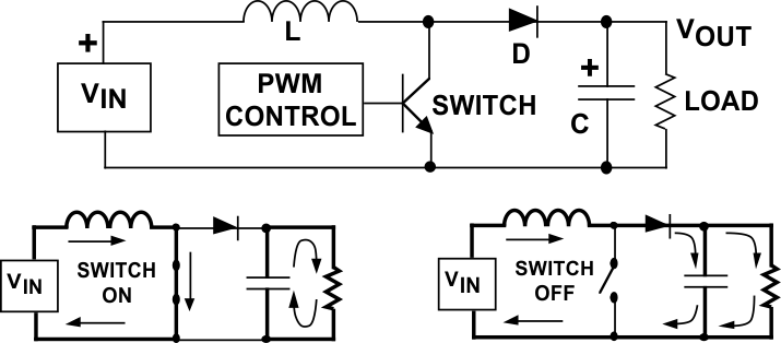
boost_regulator_snva559.gifFigure 7. Boost Regulator

Whenever the switch is on, the input voltage is forced across the inductor which causes the current through it to increase (ramp up).

When the switch is off, the decreasing inductor current forces the switch end of the inductor to swing positive. This forward biases the diode, allowing the capacitor to charge up to a voltage that is higher than the input voltage.

During steady-state operation, the inductor current flows into both the output capacitor and the load during the switch OFF time. When the switch is on, the load current is supplied only by the capacitor.