SNVA559C September 2012 – February 2019 LM2574 , LM2575-N , LM2575HV , LM2576 , LM2576HV , LM2577
-
Switching regulator fundamentals
- Trademarks
- 1 Switching Fundamentals
- 2 Switching Converter Topologies
- 3 Application Hints for Switching Regulators
- 4 Application Circuits
- 5 References and Related Products
- Revision History
3.2 Proper Grounding
The ground in a circuit is supposed to be at one potential, but in real life it is not. When ground currents flow through traces which have non-zero resistance, voltage differences will result at different points along the ground path.
In DC or low-frequency circuits, ground management is comparatively simple: the only parameter of critical importance is the DC resistance of a conductor, because that defines the voltage drop across it for a given current. In high-frequency circuits, it is the inductance of a trace or conductor that is much more important.
In switching converters, peak currents flow in high-frequency (> 50 kHz) pulses, which can cause severe problems if trace inductance is high. Much of the ringing and spiking seen on voltage waveforms in switching converters is the result of high current being switched through parasitic trace (or wire) inductance.
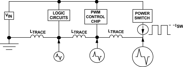
Current switching at high frequencies tends to flow near the surface of a conductor (this is called skin effect), which means that ground traces must be very wide on a PCB to avoid problems. It is usually best (when possible) to use one side of the PCB as a ground plane. Figure 17 illustrates an example of a terrible layout:
 Figure 17. Example of Poor Grounding
 The layout shown has the high-power switch return current passing through a trace that also provides the return for the PWM chip and the logic circuits. The switching current pulses flowing through the trace will cause a voltage spike (positive and negative) to occur as a result of the rising and falling edge of the switch current. This voltage spike follows directly from the v = L (di/dt) law of inductance.
It is important to note that the magnitude of the spike will be different at all points along the trace, being largest near the power switch. Taking the ground symbol as a point of reference, this shows how all three circuits would be bouncing up and down with respect to ground. More important, they would also be moving with respect to each other.
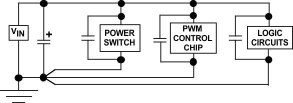
Misoperation often occurs when sensitive parts of the circuit rattle up and down due to ground switching currents. This can induce noise into the reference used to set the output voltage, resulting in excessive output ripple. Very often, regulators that suffer from ground noise problems appear to be unstable, and break into oscillations as the load current is increased (which increases ground currents). A much better layout is shown in Figure 18.
 Figure 18. Example of Good Grounding
 A big improvement is made by using single-point grounding. A good high-frequency electrolytic capacitor (like solid Tantalum) is used near the input voltage source to provide a good ground point.
All of the individual circuit elements are returned to this point using separate ground traces. This prevents high current ground pulses from bouncing the logic circuits up and down.
Another important improvement is that the power switch (which has the highest ground pin current) is placed as close as possible to the input capacitor. This minimizes the trace inductance along its ground path.
It should also be pointed out that all of the individual circuit blocks have local bypass capacitors tied directly across them. The purpose of this capacitor is RF bypass, so it must be a ceramic or film capacitor (or both).
A good value for bypassing logic devices would be 0.01-μF ceramic capacitor(s), distributed as required.
If the circuit to be bypassed generates large current pulses (like the power switch), more capacitance is required. A good choice would be an aluminum electrolytic bypassed with a film and ceramic capacitor. Exact size depends on peak current, but the more capacitance used, the better the result.