SNVA559C September 2012 – February 2019 LM2574 , LM2575-N , LM2575HV , LM2576 , LM2576HV , LM2577
-
Switching regulator fundamentals
- Trademarks
- 1 Switching Fundamentals
- 2 Switching Converter Topologies
- 3 Application Hints for Switching Regulators
- 4 Application Circuits
- 5 References and Related Products
- Revision History
4.3 LM2577 Three-Output, Isolated Flyback Regulator
Many applications require electrical isolation between the input and output terminals of the power supply (for example, medical monitoring instruments require isolation to assure patient safety).
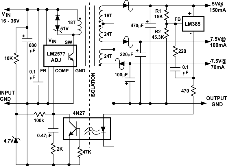
Figure 28 shows an example of a three-output flyback regulator 2 built using the LM2577 that has electrical isolation between the input and output voltages.
 Figure 28. Three-Output Isolated Flyback Regulator
 Three output voltages are obtained from three separate transformer secondary windings, with voltage feedback being taken from the 5-V output.
To maintain electrical isolation, the feedback path uses a 4N27 opto-coupler to transfer the feedback signal across the isolation barrier.
The 5-V output is regulated using an LM385 adjustable reference, whose voltage is set by R1 and R2. The LM385 operates by forcing a 1.24-V reference voltage between the positive terminal and the feedback pin, so the set voltage across the LM385 is given by:
For the values shown in this example, the voltage will be 5 V.
The function of the LM385 in the circuit can be described as an ideal Zener diode, because the current flowing through the LM385 is very small until the voltage at its positive terminal reaches 5 V with respect to ground. At that point, it tries to regulate its positive terminal to 5 V by conducting current (which flows out of the negative terminal of the LM385 and through the 470-Ω resistor into the diode side of the opto-coupler).
When the LM385 starts conducting current through the opto-coupler diode, the collector of the transistor in the opto-coupler pulls down on the compensation pin of the LM2577, which reduces the duty cycle (pulse widths) of the switching converter. In this way, a negative feedback loop is established which holds the output at 5 V.
The feedback signal from the collector of the opto-coupler is fed into the compensation pin (not the feedback pin) of the LM2577 in order to bypass the internal error amplifier of the LM2577. The gain of the LM385 is so high that using the error amplifier inside the loop would make it difficult to stabilize (and is not necessary for good performance).
Test data taken with the input voltage set to 26 V and all outputs fully loaded showed the frequency response of the control loop had a 0-dB crossover point of 1 kHz with a phase margin of 90°.
The 7.5-V and –7.5-V outputs are not directly regulated, which means their voltages are set by the pulse width of the regulated (5 V) winding. As a result, the load regulation of these two outputs is not quite as good as the 5-V output.
Table 1. Summary of Test Performance Data
| OUTPUT VOLTAGES | LINE REGULATION
(AT FULL LOAD) |
LOAD REGULATION
(VIN = 26 V) |
OUTPUT RIPPLE VOLTAGE (25°C) |
|---|---|---|---|
| 5 V | 0.2% | 0.04% (30 mA - 150 mA) | 50 mV |
| 7.5 V | 0.3% | 3% (20 mA - 100 mA) | 50 mV |
| –7.5 V | 0.3% | 2% (12 mA - 70 mA) | 50 mV |