SNVA559C September 2012 – February 2019 LM2574 , LM2575-N , LM2575HV , LM2576 , LM2576HV , LM2577
-
Switching regulator fundamentals
- Trademarks
- 1 Switching Fundamentals
- 2 Switching Converter Topologies
- 3 Application Hints for Switching Regulators
- 4 Application Circuits
- 5 References and Related Products
- Revision History
4.1.1 Increasing Available Load Power in an LM2577 Boost Regulator
One of the most frequently requested circuits is a method to squeeze more power out of a boost converter. The maximum load power available at the output is directly related to the input power available to the DC/DC converter.
When the input voltage is a low value (like 5 V), this greatly reduces the amount of power that can be drawn from the source (because the maximum input current is limited by what the switch can handle). In the case of the LM2577, the maximum switch current is 3-A (peak).
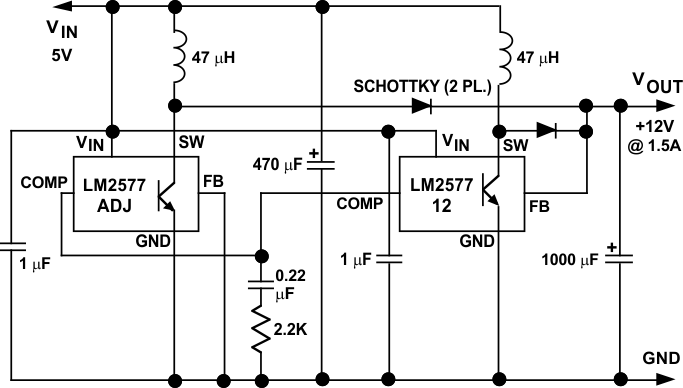
Increased load power can be obtained with the LM2577 by paralleling two devices (see Figure 26). Because current-mode control is used in the LM2577, the two converters will automatically share the load current demand.
 Figure 26. Dual LM2577 Boost Circuit
 The right-hand regulator (which is a fixed 12-V version) is the master that sets the duty cycle of both regulators (tying the Compensation pins together forces the duty cycles to track).
The master regulator has direct feedback from the output, while the other regulator has its Feedback pin grounded. Grounding the Feedback pin makes the regulator attempt to run wide open (at maximum duty cycle), but the master regulator controls the voltage at both Compensation pins, which adjusts the pulse widths as required to hold the output voltage at 12 V.