SNVA559C September 2012 – February 2019 LM2574 , LM2575-N , LM2575HV , LM2576 , LM2576HV , LM2577
-
Switching regulator fundamentals
- Trademarks
- 1 Switching Fundamentals
- 2 Switching Converter Topologies
- 3 Application Hints for Switching Regulators
- 4 Application Circuits
- 5 References and Related Products
- Revision History
2.9 Half-Bridge Converter
The Half-Bridge is a two-transistor converter frequently used in high-power designs. It is well-suited for applications requiring load power in the range of 50 0W to 1500 W, and is almost always operated directly from the AC line.
Offline operation means that no large 60-Hz power transformer is used, eliminating the heaviest and costliest component of a typical transformer-powered supply. All of the transformers in the half-bridge used for power conversion operate at the switching frequency (typically 50 kHz or higher) which means they can be very small and efficient.
A very important advantage of the half-bridge is input-to-output isolation (the regulated DC output is electrically isolated from the AC line). But, this means that all of the PWM control circuitry must be referenced to the DC output ground.
The voltage to run the control circuits is usually generated from a DC rail that is powered by a small 60-Hz transformer feeding a three-terminal regulator. In some designs requiring extremely high efficiency, the switcher output takes over and provides internal power after the start-up period.
The switch transistor drive circuitry must be isolated from the transistors, requiring the use of base drive transformers. The added complexity of the base drive circuitry is a disadvantage of using the half-bridge design.
If a 230 VAC line voltage is rectified by a full-wave bridge and filtered by a capacitor, an unregulated DC voltage of about 300 V will be available for DC/DC conversion. If 115 VAC is used, a voltage doubler circuit is typically used to generate the 300-V rail.
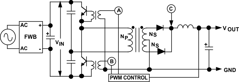
 Figure 13. Half-Bridge Converter
 The basic half-bridge converter is shown in Figure 13. A capacitive divider is tied directly across the unregulated DC input voltage, providing a reference voltage of 1/2 VIN for one end of the transformer primary winding. The other end of the primary is actively driven up and down as the transistors alternately turn on and off.
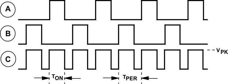
The switch transistors force one-half of the input voltage across the primary winding during the switch on time, reversing polarity as the transistors alternate. The switching transistors are never on at the same time, or they would be destroyed (because they are tied directly across VIN). The timing diagram for the half-bridge converter is shown in Figure 14 (it is the same as the push-pull).
When the A transistor is on, a dot-positive voltage is forced across the primary winding and reflected on the secondary side (with the magnitude being set by the transformer turns ratio). The dot-positive secondary voltage turns on the upper rectifier diode, supplying current to both the output capacitor and the load.
When the A transistor turns off and the B transistor turns on, the polarity of the primary voltage is reversed. The secondary voltage polarity is also reversed, turning on the lower diode (which supplies current to the output capacitor and the load).
In a Half-Bridge converter, primary and secondary current flow in the transformer at the same time (when either transistor is on), supplying the load current and charging the output capacitor. The output capacitor discharges into the load only during the time when both transistors are off.
 Figure 14. Timing Diagram for Half-Bridge Converter
 It can be seen that the voltage pulses on the transformer secondary side (applied to the L-C filter) are occurring at twice the frequency of the PWM converter which supplies the drive pulses for the switching transistors.
The output voltage is again given by Equation 4:
The peak amplitude of the secondary pulses (VPK) is given by Equation 5: