SNVA559C September 2012 – February 2019 LM2574 , LM2575-N , LM2575HV , LM2576 , LM2576HV , LM2577
-
Switching regulator fundamentals
- Trademarks
- 1 Switching Fundamentals
- 2 Switching Converter Topologies
- 3 Application Hints for Switching Regulators
- 4 Application Circuits
- 5 References and Related Products
- Revision History
4.2 LM2577 Negative Buck Regulator
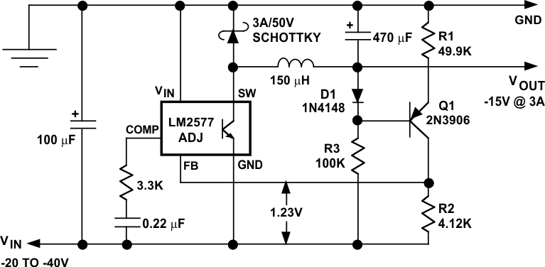
The LM2577 can be used in a Buck regulator configuration that takes a negative input voltage and produces a regulated negative output voltage (see Figure 27).
 Figure 27. Negative Buck Regulator
 The LM2577 is referenced to the negative input, which means the feedback signal coming from the regulated output must be DC level shifted. R1, D1, and Q1 form a current source that sets a current through R2 that is directly proportional to the output voltage (D1 is included to cancel out the VBE of Q1).
Neglecting the base current error of Q1, the current through R2 is equal to:
The voltage across R2 provides the 1.23-V feedback signal which the LM2577 requires for its feedback loop.
The operation of the power converter is similar to what was previously described for the Buck regulator:
- When the switch is ON, current flows from ground through the load, into the regulator output, through the inductor, and down through the switch to return to the negative input. The output capacitor also charges during the switch ON time.
- When the switch turns OFF, the voltage at the diode end of the inductor flies positive until the Schottky diode turns on (this allows the inductor current to continue to flow through the load during the OFF time). The output capacitor also discharges through the load during the OFF time, providing part of the load current.