SBVA093 December 2022 LP2992 , TPS786 , TPS7A30 , TPS7A3001-EP , TPS7A33 , TPS7A39 , TPS7A4501-SP , TPS7A47 , TPS7A47-Q1 , TPS7A4701-EP , TPS7A49 , TPS7A52 , TPS7A52-Q1 , TPS7A53 , TPS7A53-Q1 , TPS7A53A-Q1 , TPS7A53B , TPS7A54 , TPS7A54-Q1 , TPS7A57 , TPS7A7100 , TPS7A7200 , TPS7A7300 , TPS7A80 , TPS7A8300 , TPS7A83A , TPS7A84 , TPS7A84A , TPS7A85 , TPS7A85A , TPS7A87 , TPS7A89 , TPS7A90 , TPS7A91 , TPS7A92 , TPS7A94 , TPS7A96 , TPS7B7702-Q1 , TPS7H1111-SEP , TPS7H1111-SP , TPS7H1210-SEP
6.1 TPS7A57
Three parallel TPS7A57 LDO's were configured for 0.75 VDC output voltage, supplying a combined 13.2 A load current, with a maximum current imbalance of 1 A (). The TPS7A57 reference voltage is generated using a precision current source and an external resistor see reference [2]. Thus, from Section 3.1 we tie the individual reference voltage pins together to reduce the current sharing imbalance among the three LDO's. The remaining error voltage is a function of the line regulation, load regulation and offset voltage variation. Per the TPS7A57 data sheet, the line regulation is 10 nV/V, the load regulation is 175 µV/A and the offset voltage is ± 2 mV. The offset voltage dominates the total error voltage so we will set VE = ± 2 mV in the analysis. From Equation 9, RB = 4 mΩ. From Section 3, the highest load current for one LDO is when VE is positive for one and negative for the rest. From Equation 10 we conclude IOUT1 = 5.07 A and IOUT2 = IOUT3 = 4.07 A. We can determine the lowest load for an LDO by assuming one LDO has -VE while the others have +VE. From Equation 10 we conclude IOUT1 = 3.73 A and IOUT2 = IOUT3 = 4.73 A.
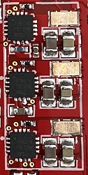
 Figure 6-1 3 Parallel TPS7A57 LDO's. The
Parallel Circuitry is Boxed in White.
Figure 6-1 3 Parallel TPS7A57 LDO's. The
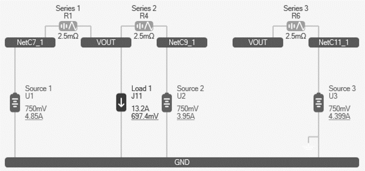
Parallel Circuitry is Boxed in White.The parallel LDO’s were implemented onto a PCB and a post route simulation was performed (Figure 6-2). The simulation assumed an ideal VOUT = 0.75 V and RB = 2.5 mΩ for each converter. The simulation results demonstrate the impact of PCB impedance mismatch from each LDO output to the load on the current sharing. Measurements versus simulation data in this configuration show strong correlation (Table 6-1) with the difference due to the slight variation of VOUT and RB in the fabricated design compared to the ideal values used in the simulation.
 Figure 6-2 Post Route Simulation of the
Parallel TPS7A57 Design
Figure 6-2 Post Route Simulation of the
Parallel TPS7A57 Design| PDN Simulation | Measurement | Error | |
|---|---|---|---|
| IOUT1 | 3.95 A | 3.99 A | 1% |
| IOUT2 | 4.399 A | 4.42 A | 0.48% |
| IOUT3 | 4.85 A | 4.79 A | 1.2% |