SBVA093 December 2022 LP2992 , TPS786 , TPS7A30 , TPS7A3001-EP , TPS7A33 , TPS7A39 , TPS7A4501-SP , TPS7A47 , TPS7A47-Q1 , TPS7A4701-EP , TPS7A49 , TPS7A52 , TPS7A52-Q1 , TPS7A53 , TPS7A53-Q1 , TPS7A53A-Q1 , TPS7A53B , TPS7A54 , TPS7A54-Q1 , TPS7A57 , TPS7A7100 , TPS7A7200 , TPS7A7300 , TPS7A80 , TPS7A8300 , TPS7A83A , TPS7A84 , TPS7A84A , TPS7A85 , TPS7A85A , TPS7A87 , TPS7A89 , TPS7A90 , TPS7A91 , TPS7A92 , TPS7A94 , TPS7A96 , TPS7B7702-Q1 , TPS7H1111-SEP , TPS7H1111-SP , TPS7H1210-SEP
6.2 TPS7A47xx
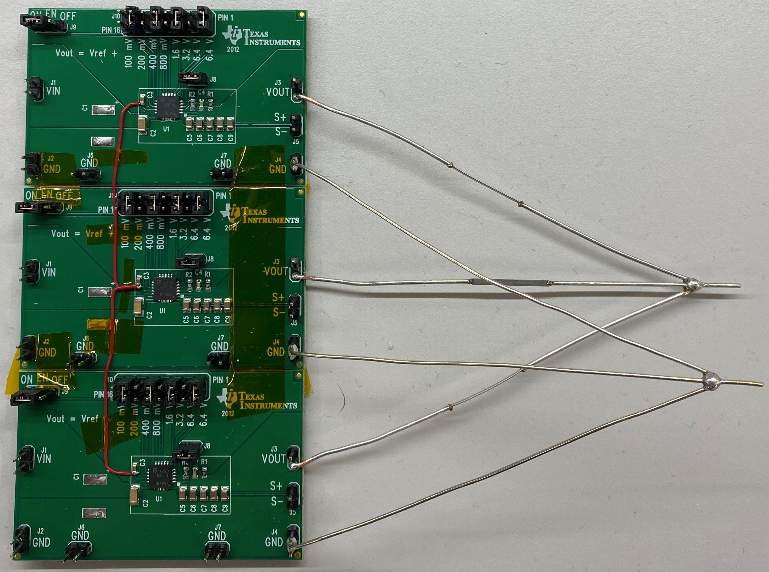
Three parallel TPS7A47 LDO's were configured for 12 VDC output voltage, supplying a combined 2.5 A load current, with a 60 mV maximum increase in load regulation (Figure 6-3). The TPS7A47 reference voltage is generated using a precision voltage source and is buffered with an internal unity gain amplifier see reference [3]. Thus, from Section 3.1 we tie the individual reference voltage pins together to reduce the current sharing imbalance among the three LDO's. The remaining error voltage is a function of the line regulation, load regulation and offset voltage variation. For the TPS7A47, the offset voltage across line and load is ± 4 mV worst case. We will set VE = ± 4 mV in the analysis and from see reference [6], RB = 61 mΩ. From Section 3, the highest load current for one LDO is when VE is positive for one and negative for the rest. From Equation 10 we conclude IOUT1 = 928 mA and IOUT2 = IOUT3 = 797 mA. We can determine the lowest load for an LDO by assuming one LDO has -VE while the others have +VE. From Equation 10 we conclude IOUT1 = 753.5 mA and IOUT2 = IOUT3 = 885 mA.
 Figure 6-3 3 Parallel TPS7A47 LDO's. Input
Supplies and 2.5 A Load not Shown.
Figure 6-3 3 Parallel TPS7A47 LDO's. Input
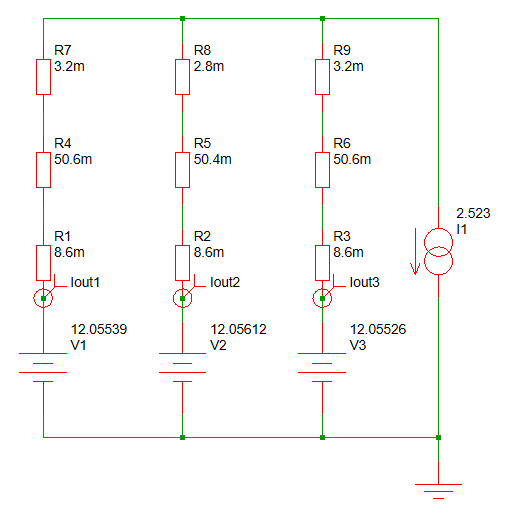
Supplies and 2.5 A Load not Shown.The parallel LDO’s were implemented using EVM's and a post route simulation of the EVM identified 8.6 mΩ in the forward and return paths. Thus a 50 mΩ discrete ballast resistor was used for each LDO. Each output voltage was measured at VIN = 15 V prior to connecting the EVM's together. Milliohm measurements were made of each ballast resistor (R4, R5 and R6) and the wire used to connect each EVM together (R7, R8 and R9), and these values were included in the spice simulation (Figure 6-4). Measurements versus simulation data in this configuration show strong correlation (Table 6-2).
 Figure 6-4 Spice Simulation of the Parallel
TPS7A47 LDOs.
Figure 6-4 Spice Simulation of the Parallel
TPS7A47 LDOs.| +/- 1 sigma Analysis, RB = 61 mΩ | +/- 6 sigma Analysis, RB = 61 mΩ | Spice Simulation | Measurement | Spice Simulation vs Measurement Error | |
|---|---|---|---|---|---|
| IOUT1 | 856 mA / 826 mA | 928 mA / 753.5 mA | 835 mA | 835 mA | 0% |
| IOUT2 | 856 mA / 826 mA | 928 mA / 753.5 mA | 855 mA | 853 mA | 0.23% |
| IOUT3 | 856 mA / 826 mA | 928 mA / 753.5 mA | 833 mA | 835 mA | 0.25% |