SBVA093 December 2022 LP2992 , TPS786 , TPS7A30 , TPS7A3001-EP , TPS7A33 , TPS7A39 , TPS7A4501-SP , TPS7A47 , TPS7A47-Q1 , TPS7A4701-EP , TPS7A49 , TPS7A52 , TPS7A52-Q1 , TPS7A53 , TPS7A53-Q1 , TPS7A53A-Q1 , TPS7A53B , TPS7A54 , TPS7A54-Q1 , TPS7A57 , TPS7A7100 , TPS7A7200 , TPS7A7300 , TPS7A80 , TPS7A8300 , TPS7A83A , TPS7A84 , TPS7A84A , TPS7A85 , TPS7A85A , TPS7A87 , TPS7A89 , TPS7A90 , TPS7A91 , TPS7A92 , TPS7A94 , TPS7A96 , TPS7B7702-Q1 , TPS7H1111-SEP , TPS7H1111-SP , TPS7H1210-SEP
4.2 PCB Ballast Resistor Design vs. Discrete Ballast Resistance
A ballast resistor can be a discrete component or the parasitic resistance of a PCB trace could be used when the ballast resistance is very small see reference [1]. In general, PCB trace resistors favor applications which are low cost and which operate in a narrow temperature range or experience very high temperatures. Discrete resistors favor applications which require maximum performance (where output voltage tolerance and transient responses are critical). Designing with a discrete ballast resistor becomes challenging when ambient temperatures exceed 125°C.
Formulas are provided in see reference [1] to determine the cross section in square mils and the PCB trace length. Here, I is the current in amperes, A is the cross section in square mils, ∆T is the change in temperature in Celsius, k is a constant such that it is 0.048 for outer layers or 0.024 for inner layers, l is the length of the trace, R is the resistance in ohms, α is the temperature coefficient of copper (3.9 x 10⁻³ (°C-1)), TA is the ambient temperature, and p is the resistivity of copper (1.74 x 10⁻⁸ (Ω⋅m)). The cross-sectional area A is a function of copper trace height (or copper weight) and copper trace width.
When designing a PCB trace resistor, limit ∆T to the maximum rise above the board temperature that the PCB can withstand. For instance, when the board material is FR4, the glass transition temperature TG is 135°C for standard FR4 and at least 175°C for high TG FR4. The board temperature as seen by the PCB ballast resistor should consider any thermal spreading of heat generated by the voltage regulator or surrounding circuitry. Thus, setting ∆T to 20°C is a common value where the LDO's can reach a junction temperature of 150°C and high TG FR4 is used. Thus, setting ∆T to 20°C is a common value where the LDO's can reach a junction temperature of 150°C and high TG FR4 is used.
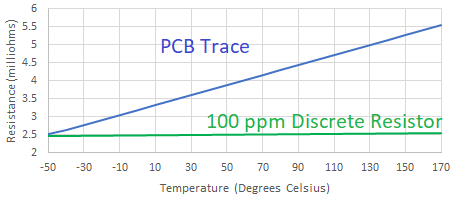
Calculate Equation 11 from the allowable temperature rise, then determine the length of the PCB trace resistor from Equation 12 and the desired PCB trace resistance. The trace length should always be calculated at the coldest temperature the trace will experience as this provides the lowest ballast resistance (Figure 4-1). Once the PCB trace length is obtained, use Equation 13 to obtain the PCB trace resistance at the maximum operating temperature of the PCB trace. Thus, the minimum and maximum PCB trace resistance is now known. The parallel voltage regulator design must then be reviewed for both values of ballast resistance. Use Equation 4 or Equation 9 to ensure IOUTn does not exceed the LDO internal current limit, and Equation 6 to assess for regulation band compliance. If the PCB trace resistance does not meet the system requirements a discrete ballast resistor can be used since they tend to vary much less across temperature (Figure 4-1).
 Figure 4-1 Tolerance Comparison
of PCB Trace and a 100 ppm Discrete Resistor Over
Temperature
Figure 4-1 Tolerance Comparison
of PCB Trace and a 100 ppm Discrete Resistor Over
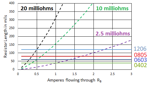
TemperatureFigure 4-2 compares discrete versus PCB trace ballast resistor techniques to show that as current increases, the PCB trace length is much larger than comparable discrete resistors. Parasitic inductance of the PCB trace may also hinder performance of the LDO during transient conditions.
 Figure 4-2 Length Comparison of
PCB Trace Resistors (Dashed Lines) Versus Discrete Resistor Packages
(Solid Lines) at Room Temperature for ∆T = 20°C
Figure 4-2 Length Comparison of
PCB Trace Resistors (Dashed Lines) Versus Discrete Resistor Packages
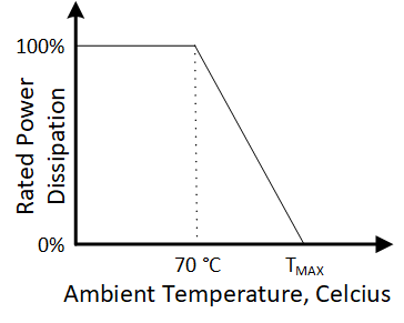
(Solid Lines) at Room Temperature for ∆T = 20°CIf a discrete resistor is chosen, the power derating curve must be reviewed if the resistor temperature exceeds 70°C (Figure 4-3). At high values of current, the power derating curve may push the resistor into a larger size package.
 Figure 4-3 Typical Discrete
Resistor Derating Curve Across Temperature