ZHCSHO9P July 2006 – February 2018 TLK2711-SP
PRODUCTION DATA.
- 1 特性
- 2 应用
- 3 说明
- 4 修订历史记录
- 5 说明 (续)
- 6 Pin Configuration and Functions
-
7 Specifications
- 7.1 Absolute Maximum Ratings
- 7.2 ESD Ratings
- 7.3 Recommended Operating Conditions
- 7.4 Thermal Information
- 7.5 TTL Input Electrical Characteristics
- 7.6 Transmitter/Receiver Electrical Characteristics
- 7.7 Reference Clock (TXCLK) Timing Requirements
- 7.8 TTL Output Switching Characteristics
- 7.9 Typical Characteristics
-
8 Detailed Description
- 8.1 Overview
- 8.2 Functional Block Diagram
- 8.3
Feature Description
- 8.3.1 Transmit Interface
- 8.3.2 Transmit Data Bus
- 8.3.3 Data Transmission Latency
- 8.3.4 8-Bit/10-Bit Encoder
- 8.3.5 Pseudo-Random Bit Stream (PRBS) Generator
- 8.3.6 Parallel to Serial
- 8.3.7 High-Speed Data Output
- 8.3.8 Receive Interface
- 8.3.9 Receive Data Bus
- 8.3.10 Data Reception Latency
- 8.3.11 Serial to Parallel
- 8.3.12 Comma Detect and 8-Bit/10-Bit Decoding
- 8.3.13 LOS Detection
- 8.3.14 PRBS Verification
- 8.3.15 Reference Clock Input
- 8.3.16 Operating Frequency Range
- 8.3.17 Testability
- 8.3.18 Loopback Testing
- 8.3.19 BIST
- 8.3.20 Power-On Reset
- 8.4 Device Functional Modes
- 9 Application and Implementation
- 10Power Supply Recommendations
- 11Layout
- 12器件和文档支持
- 13机械、封装和可订购信息
8.3.20 Power-On Reset
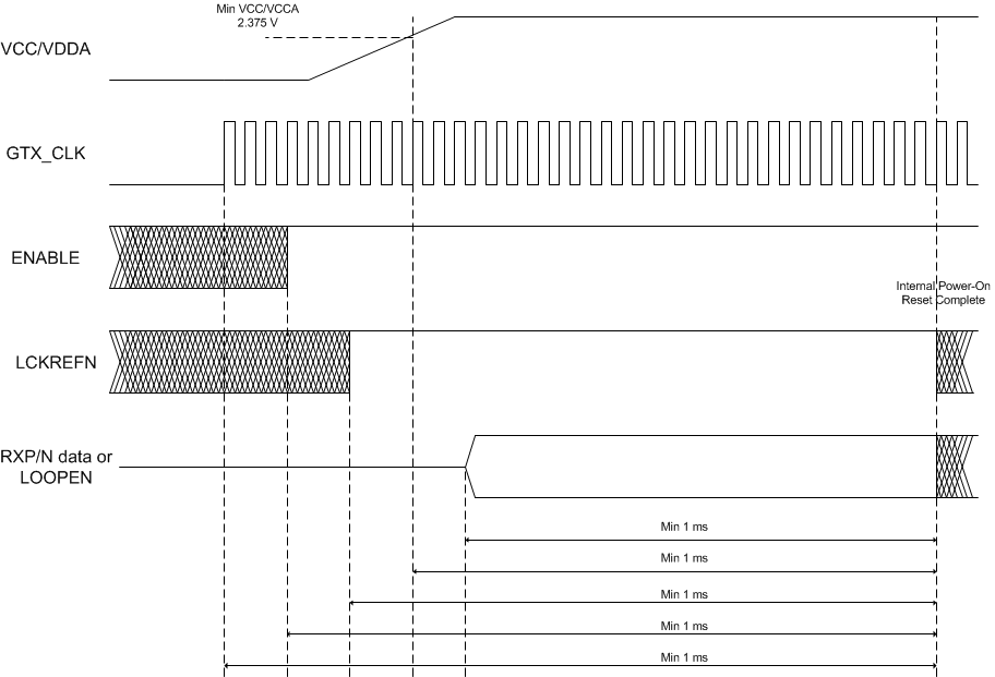
Upon application of minimum valid power and valid GTX_CLK with device enabled (ENABLE = HIGH), the TLK2711-SP generates a power-on reset. During the power-on reset the RXD0 to RXD15, RKLSB, and RKMSB signal pins go to a high-impedance state. The RXCLK is held low. LCKREFN must be deasserted (logic high state) with active transitions on the receiver during the power-on reset period. Active transitions on receiver can be accomplished with transitions on RXP/N or by assertion of LOOPEN. For TX-only applications, LOOPEN and LCKREFN can be driven logic high together. The receiver circuit requires this to properly reset. After power-up reset period, LCKREFN can be asserted for transmit only applications. The length of the power-on reset cycle depends on the TXCLK frequency, but is less than 1 ms. See Figure 12. TI recommends that the receiver be reset immediately after power up. In some conditions, it is possible for the receiver circuit to power up in state with internal contention.
If LCKREFN cannot be deasserted high during or for the complete power-on reset period, it can be deasserted high at the end of or after the power-on reset period for minimum of 1 µs with active transitions on receiver to properly complete reset of receiver.
