ZHCSHO9P July 2006 – February 2018 TLK2711-SP
PRODUCTION DATA.
- 1 特性
- 2 应用
- 3 说明
- 4 修订历史记录
- 5 说明 (续)
- 6 Pin Configuration and Functions
-
7 Specifications
- 7.1 Absolute Maximum Ratings
- 7.2 ESD Ratings
- 7.3 Recommended Operating Conditions
- 7.4 Thermal Information
- 7.5 TTL Input Electrical Characteristics
- 7.6 Transmitter/Receiver Electrical Characteristics
- 7.7 Reference Clock (TXCLK) Timing Requirements
- 7.8 TTL Output Switching Characteristics
- 7.9 Typical Characteristics
-
8 Detailed Description
- 8.1 Overview
- 8.2 Functional Block Diagram
- 8.3
Feature Description
- 8.3.1 Transmit Interface
- 8.3.2 Transmit Data Bus
- 8.3.3 Data Transmission Latency
- 8.3.4 8-Bit/10-Bit Encoder
- 8.3.5 Pseudo-Random Bit Stream (PRBS) Generator
- 8.3.6 Parallel to Serial
- 8.3.7 High-Speed Data Output
- 8.3.8 Receive Interface
- 8.3.9 Receive Data Bus
- 8.3.10 Data Reception Latency
- 8.3.11 Serial to Parallel
- 8.3.12 Comma Detect and 8-Bit/10-Bit Decoding
- 8.3.13 LOS Detection
- 8.3.14 PRBS Verification
- 8.3.15 Reference Clock Input
- 8.3.16 Operating Frequency Range
- 8.3.17 Testability
- 8.3.18 Loopback Testing
- 8.3.19 BIST
- 8.3.20 Power-On Reset
- 8.4 Device Functional Modes
- 9 Application and Implementation
- 10Power Supply Recommendations
- 11Layout
- 12器件和文档支持
- 13机械、封装和可订购信息
7.8 TTL Output Switching Characteristics
over recommended operating conditions (unless otherwise noted)| PARAMETER | TEST CONDITIONS | MIN | TYP | MAX | UNIT | |
|---|---|---|---|---|---|---|
| VOH | High-level output voltage | IOH = –2 mA, VDD = MIN | 2.1 | 2.3 | V | |
| VOL | Low-level output voltage | IOL = 2 mA, VDD = MIN | 0.25 | 0.5 | V | |
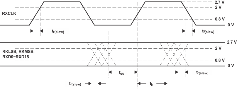
| tr(slew) | Slew rate (rising), magnitude of RXCLK, RKLSB, RKMSB, RXD0 to RXD15 | 0.8 V to 2 V, C = 5 pF, see Figure 2 | 0.5 | V/ns | ||
| tf(slew) | Slew rate (falling), magnitude of RXCLK, RKLSB, RKMSB, RXD0 to RXD15 | 0.8 V to 2 V, C = 5 pF, see Figure 2 | 0.5 | V/ns | ||
| tsu | RXD0 to RXD15, RKMSB, RKLSB setup to ↑ RXCLK | 50% voltage swing, TXCLK = 80 MHz,
see Figure 2(1) |
3 | ns | ||
| 50% voltage swing, TXCLK = 125 MHz,
see Figure 2(1) |
2.5 | |||||
| th | RXD0 to RXD15, RKMSB, RKLSB hold to ↑ RXCLK | 50% voltage swing, TXCLK = 80 MHz,
see Figure 2(1) |
3 | ns | ||
| 50% voltage swing, TXCLK = 125 MHz,
see Figure 2(1) |
2 | |||||
(1) Nonproduction tested parameters.
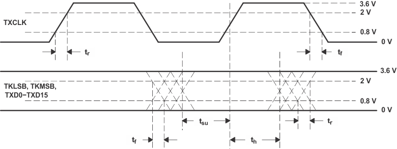
 Figure 1. TTL Data Input Valid Levels for AC Measurements
 Figure 2. TTL Data Output Valid Levels for AC Measurements
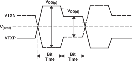
 Figure 3. Differential and Common-Mode Output Voltage
 Figure 4. Common-Mode Output Voltage Definitions