ZHCSKT9C January   2020  – March 2021 THP210

PRODUCTION DATA  

  1. 特性
  2. 应用
  3. 说明
  4. Revision History
  5. Pin Configuration and Functions
  6. Specifications
    1. 6.1 Absolute Maximum Ratings
    2. 6.2 ESD Ratings
    3. 6.3 Recommended Operating Conditions
    4. 6.4 Thermal Information
    5. 6.5 Electrical Characteristics
    6. 6.6 Typical Characteristics
  7. Parameter Measurement Information
    1. 7.1 Characterization Configuration
  8. Detailed Description
    1. 8.1 Overview
    2. 8.2 Functional Block Diagram
    3. 8.3 Feature Description
      1. 8.3.1 Super-Beta Input Bipolar Transistors
      2. 8.3.2 Power Down
      3. 8.3.3 Flexible Gain Setting
      4. 8.3.4 Amplifier Overload Power Limit
      5. 8.3.5 Unity Gain Stability
    4. 8.4 Device Functional Modes
  9. Application and Implementation
    1. 9.1 Application Information
      1. 9.1.1 I/O Headroom Considerations
      2. 9.1.2 DC Precision Analysis
        1. 9.1.2.1 DC Error Voltage at Room Temperature
        2. 9.1.2.2 DC Error Voltage Over Temperature
      3. 9.1.3 Noise Analysis
      4. 9.1.4 Mismatch of External Feedback Network
      5. 9.1.5 Operating the Power-Down Feature
      6. 9.1.6 Driving Capacitive Loads
      7. 9.1.7 Driving Differential ADCs
        1. 9.1.7.1 RC Filter Selection (Charge Kickback Filter)
        2. 9.1.7.2 Settling Time Driving the ADC Sample-and-Hold Operating Behavior
        3. 9.1.7.3 THD Performance
    2. 9.2 Typical Applications
      1. 9.2.1 MFB Filter
        1. 9.2.1.1 Design Requirements
        2. 9.2.1.2 Detailed Design Procedure
        3. 9.2.1.3 Application Curve
      2. 9.2.2 ADS891x With Single-Ended RC Filter Stage
        1. 9.2.2.1 Design Requirements
          1. 9.2.2.1.1 Measurement Results
      3. 9.2.3 Attenuation Configuration Drives the ADS8912B
        1. 9.2.3.1 Design Requirements
          1. 9.2.3.1.1 Measurement Results
  10. 10Power Supply Recommendations
  11. 11Layout
    1. 11.1 Layout Guidelines
      1. 11.1.1 Board Layout Recommendations
    2. 11.2 Layout Example
  12. 12Device and Documentation Support
    1. 12.1 Device Support
      1. 12.1.1 Development Support
    2. 12.2 Documentation Support
      1. 12.2.1 Related Documentation
    3. 12.3 接收文档更新通知
    4. 12.4 支持资源
    5. 12.5 Trademarks
    6. 12.6 静电放电警告
    7. 12.7 术语表
  13. 13Mechanical, Packaging, and Orderable Information

封装选项

机械数据 (封装 | 引脚)
散热焊盘机械数据 (封装 | 引脚)
订购信息

Settling Time Driving the ADC Sample-and-Hold Operating Behavior

The RC filter between the amplifier and the ADC helps the amplifier drive the sampling capacitor during charging (acquisition) and discharging (conversion) times. During the acquisition time, if the amplifier has a load transient at the output, the time needed to recover (or settle) is commonly defined as the settling time. Typically, to achieve minimal distortion, the end value to settle is within ½ of the ADC least significant bit (LSB).

The specified settling time of the FDA is the time required for the amplifier to recover from transients caused at the THP210 output. Although the frequency response characteristics impact the settling time of the ADC application, these characteristics are not the key element to consider. The settling time of the FDA to react to load transients depends primarily on the output impedance of the amplifier at the required signal bandwidth. Equation 5 calculates the settling time, considering the time constant of the RC combination:
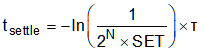
Equation 5. GUID-20200806-CA0I-3XTD-D46Z-GDQLF7ZJVZ6V-low.gif

where:

  • N is the number of bits in the ADC application
  • τ equals RF × CF
  • SET = 2 for a settling of ½ LSB, SET = 4 for a settling of ¼ LSB, and so on.

In order to verify whether the chosen RC filter combination fulfills the settling behavior, simulate the desired circuit with TINA-TI™ simulation software.