ZHCSKT9C January 2020 – March 2021 THP210
PRODUCTION DATA
- 1 特性
- 2 应用
- 3 说明
- 4 Revision History
- 5 Pin Configuration and Functions
- 6 Specifications
- 7 Parameter Measurement Information
- 8 Detailed Description
-
9 Application and Implementation
- 9.1 Application Information
- 9.2 Typical Applications
- 10Power Supply Recommendations
- 11Layout
- 12Device and Documentation Support
- 13Mechanical, Packaging, and Orderable Information
7.1 Characterization Configuration
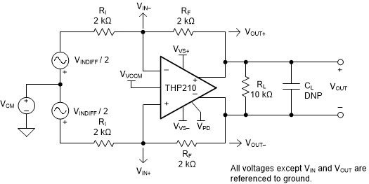
The THP210 is a fully differential amplifier (FDA) configuration that offers high dc precision, very low noise and harmonic distortion in a single, low-power amplifier. The FDA is a flexible device where the main aim is to provide a purely differential output signal centered on a user-configurable, common-mode voltage that is usually matched to the input common-mode voltage required by an analog-to-digital converter (ADC). The circuit used for characterization of the differential-to-differential performance is seen in Figure 7-1
 Figure 7-1 Differential Source to a Differential Gain of a 1-V/V Test Circuit
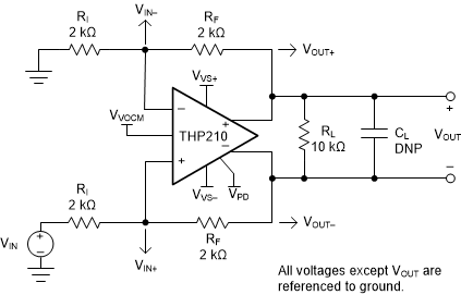
A similar circuit is used for single-ended to differential measurements, as shown in Figure 7-2.
 Figure 7-2 Single-ended Source to Differential Gain of 1-V/V Test Circuit
The characterization plots fix the RF (RF1 = RF2) value at 2 kΩ, unless otherwise noted. This value can be adjusted to match the system design parameters with the following considerations in mind:
- The current required to drive RF from the peak output voltage to the input common-mode voltage add to the overall output load current. If the total current (current through RF + current through RL) exceeds the current limit conditions, the device enters a current limit, causing the output voltage to collapse.
- High feedback resistor values (RF > 100 kΩ) interact with the amplifier input capacitance to create a zero in the feedback network. Compensation must be added to account for potential source of instability; see the TI Precision Labs FDA Stability Training for guidance on designing an appropriate compensation network.