ZHCSKT9C January   2020  – March 2021 THP210

PRODUCTION DATA  

  1. 特性
  2. 应用
  3. 说明
  4. Revision History
  5. Pin Configuration and Functions
  6. Specifications
    1. 6.1 Absolute Maximum Ratings
    2. 6.2 ESD Ratings
    3. 6.3 Recommended Operating Conditions
    4. 6.4 Thermal Information
    5. 6.5 Electrical Characteristics
    6. 6.6 Typical Characteristics
  7. Parameter Measurement Information
    1. 7.1 Characterization Configuration
  8. Detailed Description
    1. 8.1 Overview
    2. 8.2 Functional Block Diagram
    3. 8.3 Feature Description
      1. 8.3.1 Super-Beta Input Bipolar Transistors
      2. 8.3.2 Power Down
      3. 8.3.3 Flexible Gain Setting
      4. 8.3.4 Amplifier Overload Power Limit
      5. 8.3.5 Unity Gain Stability
    4. 8.4 Device Functional Modes
  9. Application and Implementation
    1. 9.1 Application Information
      1. 9.1.1 I/O Headroom Considerations
      2. 9.1.2 DC Precision Analysis
        1. 9.1.2.1 DC Error Voltage at Room Temperature
        2. 9.1.2.2 DC Error Voltage Over Temperature
      3. 9.1.3 Noise Analysis
      4. 9.1.4 Mismatch of External Feedback Network
      5. 9.1.5 Operating the Power-Down Feature
      6. 9.1.6 Driving Capacitive Loads
      7. 9.1.7 Driving Differential ADCs
        1. 9.1.7.1 RC Filter Selection (Charge Kickback Filter)
        2. 9.1.7.2 Settling Time Driving the ADC Sample-and-Hold Operating Behavior
        3. 9.1.7.3 THD Performance
    2. 9.2 Typical Applications
      1. 9.2.1 MFB Filter
        1. 9.2.1.1 Design Requirements
        2. 9.2.1.2 Detailed Design Procedure
        3. 9.2.1.3 Application Curve
      2. 9.2.2 ADS891x With Single-Ended RC Filter Stage
        1. 9.2.2.1 Design Requirements
          1. 9.2.2.1.1 Measurement Results
      3. 9.2.3 Attenuation Configuration Drives the ADS8912B
        1. 9.2.3.1 Design Requirements
          1. 9.2.3.1.1 Measurement Results
  10. 10Power Supply Recommendations
  11. 11Layout
    1. 11.1 Layout Guidelines
      1. 11.1.1 Board Layout Recommendations
    2. 11.2 Layout Example
  12. 12Device and Documentation Support
    1. 12.1 Device Support
      1. 12.1.1 Development Support
    2. 12.2 Documentation Support
      1. 12.2.1 Related Documentation
    3. 12.3 接收文档更新通知
    4. 12.4 支持资源
    5. 12.5 Trademarks
    6. 12.6 静电放电警告
    7. 12.7 术语表
  13. 13Mechanical, Packaging, and Orderable Information

封装选项

机械数据 (封装 | 引脚)
散热焊盘机械数据 (封装 | 引脚)
订购信息
Measurement Results

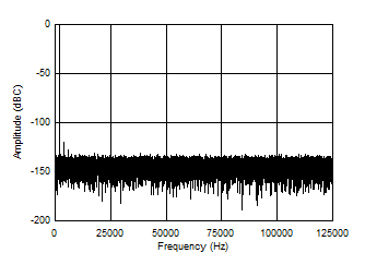
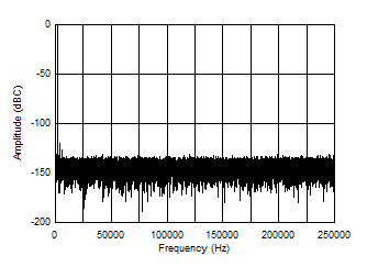
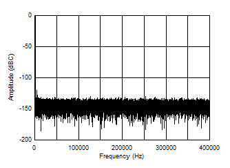
The THP210 and the filter combination listed in Section 9.2.2.1 allow for the best trade-off between harmonic distortion and maintaining stability of the FDA. Table 9-1 and Figure 9-13 through Figure 9-15 showcase the device performance.

Table 9-1 THP210 + ADS891x: FFT Data Summary
ADC VERSIONADC SPECIFICATIONSAMPLING RATESNRTHD(1) SINAD
ADS8910B1-MSPS max, 18 bit800 kSPS100.37 dB–118.4 dB100.31 dB
ADS8912B500 kSPS, 18 bit500 kSPS100.4 dB–118.44 dB100.33 dB
ADS8914B250 kSPS, 18 bit250 kSPS100.37 dB–118.72 dB100.33 dB
THD can further be improved by providing a bipolar power supply for more headroom for the negative voltage swing. In the given circuit, a negative supply of VS– = 0.23 V improved the THD to –120.5 dB.
GUID-A662CFF2-9B85-47C6-B1DF-5EBB1F751E5D-low.gif
fIN = 2 kHz, 100.37 dB SNR, –118.4 dB THD
Figure 9-13 Noise Performance FFT Plot:
THP210 + ADS8910B, 800 kSPS, 18-Bit
GUID-16B3A4E6-A552-4E0E-AE37-45A17B796C38-low.gif
fIN = 2 kHz, 100.37 dB SNR, –118.72 dB THD
Figure 9-15 Noise Performance FFT Plot:
THP210 + ADS8914B, 250 kSPS, 18-Bit
GUID-1116C04F-0798-44A7-A58B-26BC560322F6-low.gif
fIN = 2 kHz, 100.4 dB SNR, –118.44 dB THD
Figure 9-14 Noise Performance FFT Plot:
THP210 + ADS8912B, 500 kSPS, 18-Bit