ZHCSKT9C January 2020 – March 2021 THP210
PRODUCTION DATA
- 1 特性
- 2 应用
- 3 说明
- 4 Revision History
- 5 Pin Configuration and Functions
- 6 Specifications
- 7 Parameter Measurement Information
- 8 Detailed Description
-
9 Application and Implementation
- 9.1 Application Information
- 9.2 Typical Applications
- 10Power Supply Recommendations
- 11Layout
- 12Device and Documentation Support
- 13Mechanical, Packaging, and Orderable Information
9.1.2.1 DC Error Voltage at Room Temperature
Good dc linearity allows the designer to minimize the total dc output error of the system. In particular, this error divides into two contributions: the initial error at the normal operating condition of 25°C, and the drift error over temperature. The main sources of these errors typically arise from:
- Voltage error due to the input offset voltage (VIO)
- Voltage error due to noninverting and inverting bias current (IB–, IB+)
- The common-mode rejection ratio (CMRR) of the FDA
- Voltage error due to mismatch between input and output common-mode voltages (VVOCM – VICM)
One major source of error comes from the effect of mismatched resistor values and the ratios on the two sides of the FDA. For this analysis, this error term is neglected. The effects are described separately in Section 9.1.4.
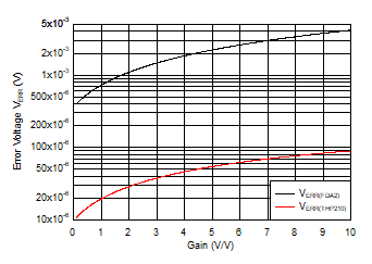
The THP210 super-beta input device features extremely-low input bias current, trimmed low input offset voltage, and the lowest offset drift over the full temperature operating range. These features allow the device to produce a negligible initial error band at 25°C, but also exceptional robust behavior over temperature. The red curve in Figure 9-1 showcases a simulation of the total dc error voltage at 25°C versus different gain configurations based on the application configuration shown in Figure 9-2.
 Figure 9-1 TINA-TI™ Software Simulation
of DC Error Voltage at Different Gain Settings (Variable R2)
 Figure 9-2 FDA DC Error Model
One use case at a differential input
voltage of VID = 200 mV and a gain of 5 V/V (that corresponds to
R2 = 5 kΩ) reveals that the initial dc error of the THP210 is 4.5 µV.
A comparable FDA2 with VIO = 200 µV,
IB = 650 nA, and IIO = 30 nA results in a 2.22-mV dc
error voltage that results in a factor of approximately 500 higher dc error.
In addition, Figure 9-3 shows that the absolute dc accuracy of the THP210 nearly adds an error voltage on the system. The dominant factors for the initial error band are mainly due to the feedback resistor mismatch that is not considered in the simulation plot.