ZHCSH08 October 2017 MSP432E411Y
PRODUCTION DATA.
- 1器件概述
- 2Revision History
- 3Device Characteristics
- 4Terminal Configuration and Functions
-
5Specifications
- 5.1 Absolute Maximum Ratings
- 5.2 ESD Ratings
- 5.3 Recommended Operating Conditions
- 5.4 Recommended DC Operating Conditions
- 5.5 Recommended GPIO Operating Characteristics
- 5.6 Recommended Fast GPIO Pad Operating Conditions
- 5.7 Recommended Slow GPIO Pad Operating Conditions
- 5.8 GPIO Current Restrictions
- 5.9 I/O Reliability
- 5.10 Current Consumption
- 5.11 Peripheral Current Consumption
- 5.12 LDO Regulator Characteristics
- 5.13 Power Dissipation
- 5.14 Thermal Resistance Characteristics, 212-Pin ZAD (NFBGA) Package
- 5.15
Timing and Switching Characteristics
- 5.15.1 Load Conditions
- 5.15.2 Power Supply Sequencing
- 5.15.3 Reset Timing
- 5.15.4
Clock Specifications
- 5.15.4.1 PLL Specifications
- 5.15.4.2 PIOSC Specifications
- 5.15.4.3 Low-Frequency Oscillator Specifications
- 5.15.4.4 Hibernation Low-Frequency Oscillator Specifications
- 5.15.4.5 Main Oscillator Specifications
- 5.15.4.6 Main Oscillator Specification WIth ADC
- 5.15.4.7 System Clock Characteristics With USB Operation
- 5.15.5 Sleep Modes
- 5.15.6 Hibernation Module
- 5.15.7 Flash Memory
- 5.15.8 EEPROM
- 5.15.9 Input/Output Pin Characteristics
- 5.15.10 External Peripheral Interface (EPI)
- 5.15.11 Analog-to-Digital Converter (ADC)
- 5.15.12 Synchronous Serial Interface (SSI)
- 5.15.13 Inter-Integrated Circuit (I2C) Interface
- 5.15.14
Ethernet Controller
- 5.15.14.1 DC Characteristics
- 5.15.14.2 Clock Characteristics for Ethernet
- 5.15.14.3
AC Characteristics
- Table 5-42 Ethernet Controller Enable and Software Reset Timing
- Table 5-43 MII Serial Management Timing
- Table 5-44 100-Mbps MII Transmit Timing
- Table 5-45 100-Mbps MII Receive Timing
- Table 5-46 100Base-TX Transmit Timing
- Table 5-47 10-Mbps MII Transmit Timing
- Table 5-48 10-Mbps MII Receive Timing
- Table 5-49 10Base-T Normal Link Pulse Timing
- Table 5-50 Auto-Negotiation Fast Link Pulse (FLP) Timing
- Table 5-51 100Base-TX Signal Detect Timing
- Table 5-52 RMII Transmit Timing
- Table 5-53 RMII Receive Timing
- 5.15.15 Universal Serial Bus (USB) Controller
- 5.15.16 LCD Controller
- 5.15.17 Analog Comparator
- 5.15.18 Pulse-Width Modulator (PWM)
- 5.15.19 Emulation and Debug
-
6Detailed Description
- 6.1 Overview
- 6.2 Functional Block Diagram
- 6.3 Arm Cortex-M4F Processor Core
- 6.4 On-Chip Memory
- 6.5
Peripherals
- 6.5.1 External Peripheral Interface (EPI)
- 6.5.2 Cyclical Redundancy Check (CRC)
- 6.5.3 Advanced Encryption Standard (AES) Accelerator
- 6.5.4 Data Encryption Standard (DES) Accelerator
- 6.5.5 Secure Hash Algorithm/Message Digest Algorithm (SHA/MD5) Accelerator
- 6.5.6 Serial Communications Peripherals
- 6.5.7 System Integration
- 6.5.8 LCD Controller
- 6.5.9 Advanced Motion Control
- 6.5.10 Analog
- 6.5.11 JTAG and Arm Serial Wire Debug
- 6.5.12 Peripheral Memory Map
- 6.6 Identification
- 6.7 Boot Modes
- 7Applications, Implementation, and Layout
- 8器件和文档支持
- 9机械、封装和可订购信息
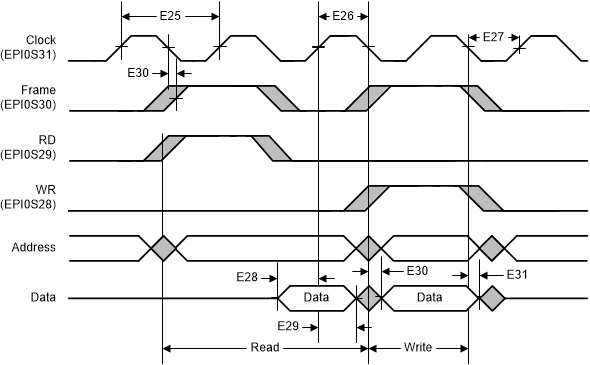
Table 5-31 EPI General-Purpose Interface Characteristics
over operating free-air temperature (unless otherwise noted) (see Figure 5-23)| NO. | PARAMETER | MIN | TYP | MAX | UNIT | |
|---|---|---|---|---|---|---|
| E25 | tCK | General-purpose clock period | 16.67 | ns | ||
| E26 | tCH | General-purpose clock high time | 8.33 | ns | ||
| E27 | tCL | General-purpose clock low time | 8.33 | ns | ||
| E28 | tISU | Input signal set up time to rising clock edge | 8.50 | ns | ||
| E29 | tIH | Input signal hold time from rising clock edge | 0 | ns | ||
| E30 | tDV | Falling clock edge to output valid | 4 | ns | ||
| E31 | tDI | Falling clock edge to output invalid | 4 | ns | ||

NOTE:
This figure shows accesses when the FRM50 bit is clear, the FRMCNT field is 0x0, and the WR2CYC bit is clear.Table 5-32 lists the switching characteristics of the PSRAM interface.