ZHCSI67D May 2018 – December 2019 MSP430FR2153 , MSP430FR2155 , MSP430FR2353 , MSP430FR2355
PRODUCTION DATA.
- 1器件概述
- 2Device Comparison
- 3Terminal Configuration and Functions
-
4Specifications
- 4.1 Absolute Maximum Ratings
- 4.2 ESD Ratings
- 4.3 Recommended Operating Conditions
- 4.4 Active Mode Supply Current Into VCC Excluding External Current
- 4.5 Active Mode Supply Current Per MHz
- 4.6 Low-Power Mode LPM0 Supply Currents Into VCC Excluding External Current
- 4.7 Low-Power Mode LPM3 and LPM4 Supply Currents (Into VCC) Excluding External Current
- 4.8 Low-Power Mode LPMx.5 Supply Currents (Into VCC) Excluding External Current
- 4.9 Production Distribution of LPM Supply Currents
- 4.10 Typical Characteristics - Current Consumption Per Module
- 4.11 Thermal Resistance Characteristics
- 4.12
Timing and Switching Characteristics
- 4.12.1 Power Supply Sequencing
- 4.12.2 Reset Timing
- 4.12.3 Clock Specifications
- 4.12.4 Internal Shared Reference
- 4.12.5 General-Purpose I/Os
- 4.12.6 Digital I/O Typical Characteristics
- 4.12.7 Timer_B
- 4.12.8
eUSCI
- Table 4-14 eUSCI (UART Mode) Clock Frequencies
- Table 4-15 eUSCI (UART Mode) Switching Characteristics
- Table 4-16 eUSCI (SPI Master Mode) Clock Frequency
- Table 4-17 eUSCI (SPI Master Mode) Switching Characteristics
- Table 4-18 eUSCI (SPI Slave Mode) Switching Characteristics
- Table 4-19 eUSCI (I2C Mode) Switching Characteristics
- 4.12.9 ADC
- 4.12.10 Enhanced Comparator (eCOMP)
- 4.12.11 Smart Analog Combo (SAC) (MSP430FR235x Devices Only)
- 4.12.12 FRAM
- 4.12.13 Emulation and Debug
-
5Detailed Description
- 5.1 CPU
- 5.2 Operating Modes
- 5.3 Interrupt Vector Addresses
- 5.4 Memory Organization
- 5.5 Bootloader (BSL)
- 5.6 JTAG Standard Interface
- 5.7 Spy-Bi-Wire Interface (SBW)
- 5.8 FRAM
- 5.9 Memory Protection
- 5.10
Peripherals
- 5.10.1 Power Management Module (PMM) and On-Chip Reference Voltages
- 5.10.2 Clock System (CS) and Clock Distribution
- 5.10.3 General-Purpose Input/Output Port (I/O)
- 5.10.4 Watchdog Timer (WDT)
- 5.10.5 System Module (SYS)
- 5.10.6 Cyclic Redundancy Check (CRC)
- 5.10.7 Interrupt Compare Controller (ICC)
- 5.10.8 Enhanced Universal Serial Communication Interface (eUSCI_A0, eUSCI_A1, eUSCI_B0, eUSCI_B1)
- 5.10.9 Timers (Timer0_B3, Timer1_B3, Timer2_B3, Timer3_B7)
- 5.10.10 Backup Memory (BKMEM)
- 5.10.11 Real-Time Clock (RTC) Counter
- 5.10.12 12-Bit Analog-to-Digital Converter (ADC)
- 5.10.13 Enhanced Comparator
- 5.10.14 Manchester Function Module (MFM)
- 5.10.15 Smart Analog Combo (SAC) (MSP430FR235x Devices Only)
- 5.10.16 eCOMP0, eCOMP1, SAC0, SAC1, SAC2, and SAC3 Interconnection (MSP430FR235x Devices Only)
- 5.10.17 Cross-Chip Interconnection (SACx are MSP430FR235x Devices Only)
- 5.10.18 Embedded Emulation Module (EEM)
- 5.10.19 Peripheral File Map
- 5.11 Input/Output Diagrams
- 5.12 Device Descriptors (TLV)
- 5.13 Identification
- 6Applications, Implementation, and Layout
- 7器件和文档支持
- 8机械、封装和可订购信息
封装选项
机械数据 (封装 | 引脚)
散热焊盘机械数据 (封装 | 引脚)
订购信息
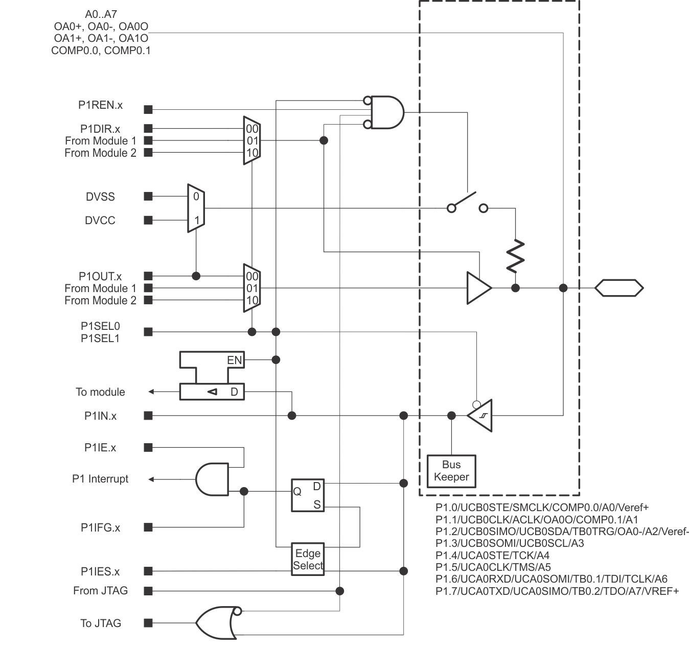
5.11.1 Port P1 Input/Output With Schmitt Trigger
Figure 5-4 shows the port diagram. Table 5-63 summarizes the selection of the port function.
 Figure 5-4 Port P1 Input/Output With Schmitt Trigger
 Table 5-63 Port P1 Pin Functions
| PIN NAME (P1.x) | x | FUNCTION | CONTROL BITS AND SIGNALS(1) | |||
|---|---|---|---|---|---|---|
| P1DIR.x | P1SELx | JTAG | ||||
| P1.0/UCB0STE/SMCLK/ COMP0.0/A0/Veref+ | 0 | P1.0 (I/O) | I: 0; O: 1 | 00 | N/A | |
| UCB0STE | X | 01 | N/A | |||
| SMCLK | 1 | 10 | N/A | |||
| VSS | 0 | |||||
| COMP0.0, A0/Veref+ | X | 11 | N/A | |||
| P1.1/UCB0CLK/ACLK/ OA0O/COMP0.1/A1 | 1 | P1.1 (I/O) | I: 0; O: 1 | 0 | N/A | |
| UCB0CLK | X | 01 | N/A | |||
| ACLK | 1 | 10 | N/A | |||
| VSS | 0 | |||||
| OA0O(2), COMP0.1, A1 | X | 11 | N/A | |||
| P1.2/UCB0SIMO/ UCB0SDA/TB0TRG/ OA0-/A2/Veref- | 2 | P1.2 (I/O) | I: 0; O: 1 | 00 | N/A | |
| UCB0SIMO/UCB0SDA | X | 01 | N/A | |||
| TB0TRG | 0 | 10 | N/A | |||
| OA0-(2), A2/Veref- | X | 11 | N/A | |||
| P1.3/UCB0SOMI/ UCB0SCL/OA0+/A3 | 3 | P1.3 (I/O) | I: 0; O: 1 | 00 | N/A | |
| UCB0SOMI/UCB0SCL | X | 01 | N/A | |||
| OA0+(2), A3 | X | 11 | N/A | |||
| P1.4/UCA0STE/TCK/A4 | 4 | P1.4 (I/O) | I: 0; O: 1 | 00 | Disabled | |
| UCA0STE | X | 01 | Disabled | |||
| A4 | X | 11 | Disabled | |||
| JTAG TCK | X | X | TCK | |||
| P1.5/UCA0CLK/TMS/ OA1O/A5 | 5 | P1.5 (I/O) | I: 0; O: 1 | 00 | Disabled | |
| UCA0CLK | X | 01 | Disabled | |||
| OA1O(2), A5 | X | 11 | Disabled | |||
| JTAG TMS | X | X | TMS | |||
| P1.6/UCA0RXD/ UCA0SOMI/TB0.1/TDI/ TCLK/OA1-/A6 | 6 | P1.6 (I/O) | I: 0; O: 1 | 00 | Disabled | |
| UCA0RXD/UCA0SOMI | X | 01 | Disabled | |||
| TB0.CCI1A | 0 | 10 | Disabled | |||
| TB0.1 | 1 | |||||
| OA1-(2), A6 | X | 11 | Disabled | |||
| JTAG TDI/TCLK | X | X | TDI/TCLK | |||
| P1.7/UCA0TXD/ UCA0SIMO/TB0.2/TDO/ OA1+/A7/VREF+ | 7 | P1.7 (I/O) | I: 0; O: 1 | 00 | Disabled | |
| UCA0TXD/UCA0SIMO | X | 01 | Disabled | |||
| TB0.CCI2A | 0 | 10 | Disabled | |||
| TB0.2 | 1 | |||||
| OA1+(2), A7, VREF+ | X | 11 | Disabled | |||
| JTAG TDO | X | X | TDO | |||
(1) X = don't care
(2) MSP430FR235x devices only