ZHCSNB5B June 2021 – February 2025 LM25148-Q1
PRODUCTION DATA
- 1
- 1 特性
- 2 应用
- 3 说明
- 4 说明(续)
- 5 可订购器件型号
- 6 引脚配置和功能
- 7 规格
-
8 详细说明
- 8.1 概述
- 8.2 功能方框图
- 8.3
特性说明
- 8.3.1 输入电压范围 (VIN)
- 8.3.2 高压偏置电源稳压器(VCC、VCCX、VDDA)
- 8.3.3 精密使能端 (EN)
- 8.3.4 电源正常监视器 (PG)
- 8.3.5 开关频率 (RT)
- 8.3.6 双随机展频 (DRSS)
- 8.3.7 软启动
- 8.3.8 输出电压设定值 (FB)
- 8.3.9 最短可控导通时间
- 8.3.10 误差放大器和 PWM 比较器(FB、EXTCOMP)
- 8.3.11 斜率补偿
- 8.3.12 电感器电流检测(ISNS+、VOUT)
- 8.3.13 断续模式电流限制
- 8.3.14 高侧和低侧栅极驱动器(HO、LO)
- 8.3.15 输出配置 (CNFG)
- 8.3.16 单输出双相运行
- 8.4 器件功能模式
- 9 应用和实施
- 10器件和文档支持
- 11修订历史记录
- 12机械、封装和可订购信息
8.3.14 高侧和低侧栅极驱动器(HO、LO)
LM25148-Q1 包含栅极驱动器和一个关联的高侧电平转换器来驱动外部 N 沟道 MOSFET。高侧栅极驱动器与内部自举二极管 DBOOT 和自举电容器 CBOOT 搭配使用。在低侧 MOSFET 的导通间隔期间,SW 电压约为 0V,而 CBOOT 通过内部 DBOOT 从 VCC 充电。TI 建议使用短迹线在 CBOOT 和 SW 引脚之间连接一个 0.1μF 陶瓷电容器。
LO 和 HO 输出由自适应死区时间方法进行控制,因此两个输出(HO 和 LO)绝不会同时启用,从而防止出现跨导。在允许启用 LO 驱动器输出之前,自适应死区时间逻辑会先禁用 HO 并等待 HO 电压降至 2V(典型值)以下。然后,会允许 LO 在短暂延迟(HO 下降至 LO 上升延迟)后启用。同样,HO 导通会延迟,直到 LO 电压降至 2V 以下。该技术可确保任何尺寸的 N 沟道功率 MOSFET 实现(包括并联 MOSFET 配置)具有足够的死区时间。
添加串联栅极电阻器时要格外小心,因为这可能影响有效死区时间。所选的高侧 MOSFET 确定了相应自举电容值 CBOOT,如方程式 12 所示。
方程式 12. 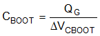
其中
- QG 是高侧 MOSFET 在适用栅极驱动电压下的总栅极电荷。
- ΔVCBOOT 是高侧 MOSFET 驱动器在导通后的电压变化。
若要确定 CBOOT,请选择合适的 ΔVCBOOT,使可用的栅极驱动电压不会受到显著影响。ΔVCBOOT 的可接受范围为 100mV 至 300mV。自举电容器必须为低 ESR 陶瓷电容器,典型值为 0.1µF。请使用具有逻辑电平栅极阈值电压的高侧和低侧 MOSFET。