ZHCSNB5A June   2021  – February 2023 LM25148-Q1

PRODUCTION DATA  

  1. 特性
  2. 应用
  3. 说明
  4. Revision History
  5. 说明(续)
  6. Pin Configuration and Functions
    1. 6.1 Wettable Flanks
  7. Specifications
    1. 7.1 Absolute Maximum Ratings
    2. 7.2 ESD Ratings 
    3. 7.3 Recommended Operating Conditions
    4. 7.4 Thermal Information
    5. 7.5 Electrical Characteristics
    6. 7.6 Typical Characteristics
  8. Detailed Description
    1. 8.1 Overview
    2. 8.2 Functional Block Diagram
    3. 8.3 Feature Description
      1. 8.3.1  Input Voltage Range (VIN)
      2. 8.3.2  High-Voltage Bias Supply Regulator (VCC, VCCX, VDDA)
      3. 8.3.3  Precision Enable (EN)
      4. 8.3.4  Power-Good Monitor (PG)
      5. 8.3.5  Switching Frequency (RT)
      6. 8.3.6  Dual Random Spread Spectrum (DRSS)
      7. 8.3.7  Soft Start
      8. 8.3.8  Output Voltage Setpoint (FB)
      9. 8.3.9  Minimum Controllable On Time
      10. 8.3.10 Error Amplifier and PWM Comparator (FB, EXTCOMP)
      11. 8.3.11 Slope Compensation
      12. 8.3.12 Inductor Current Sense (ISNS+, VOUT)
        1. 8.3.12.1 Shunt Current Sensing
        2. 8.3.12.2 Inductor DCR Current Sensing
      13. 8.3.13 Hiccup Mode Current Limiting
      14. 8.3.14 High-Side and Low-Side Gate Drivers (HO, LO)
      15. 8.3.15 Output Configurations (CNFG)
      16. 8.3.16 Single-Output Dual-Phase Operation
    4. 8.4 Device Functional Modes
      1. 8.4.1 Sleep Mode
      2. 8.4.2 Pulse Frequency Modulation and Synchronization (PFM/SYNC)
      3. 8.4.3 Thermal Shutdown
  9. Application and Implementation
    1. 9.1 Application Information
      1. 9.1.1 Power Train Components
        1. 9.1.1.1 Buck Inductor
        2. 9.1.1.2 Output Capacitors
        3. 9.1.1.3 Input Capacitors
        4. 9.1.1.4 Power MOSFETs
        5. 9.1.1.5 EMI Filter
      2. 9.1.2 Error Amplifier and Compensation
    2. 9.2 Typical Applications
      1. 9.2.1 Design 1 – High Efficiency 2.1-MHz Synchronous Buck Regulator
        1. 9.2.1.1 Design Requirements
        2. 9.2.1.2 Detailed Design Procedure
          1. 9.2.1.2.1 Custom Design with WEBENCH® Tools
          2. 9.2.1.2.2 Buck Inductor
          3. 9.2.1.2.3 Current-Sense Resistance
          4. 9.2.1.2.4 Output Capacitors
          5. 9.2.1.2.5 Input Capacitors
          6. 9.2.1.2.6 Frequency Set Resistor
          7. 9.2.1.2.7 Feedback Resistors
          8. 9.2.1.2.8 Compensation Components
        3. 9.2.1.3 Application Curves
      2. 9.2.2 Design 2 – High Efficiency 440-kHz Synchronous Buck Regulator
        1. 9.2.2.1 Design Requirements
        2. 9.2.2.2 Detailed Design Procedure
        3. 9.2.2.3 Application Curves
      3. 9.2.3 Design 3 – Dual-Phase 400-kHz 20-A Synchronous Buck Regulator
        1. 9.2.3.1 Design Requirements
        2. 9.2.3.2 Detailed Design Procedure
        3. 9.2.3.3 Application Curves
    3. 9.3 Power Supply Recommendations
    4. 9.4 Layout
      1. 9.4.1 Layout Guidelines
        1. 9.4.1.1 Power Stage Layout
        2. 9.4.1.2 Gate-Drive Layout
        3. 9.4.1.3 PWM Controller Layout
        4. 9.4.1.4 Thermal Design and Layout
        5. 9.4.1.5 Ground Plane Design
      2. 9.4.2 Layout Example
  10. 10Device and Documentation Support
    1. 10.1 Device Support
      1. 10.1.1 Development Support
        1. 10.1.1.1 Custom Design with WEBENCH® Tools
    2. 10.2 Documentation Support
      1. 10.2.1 Related Documentation
        1. 10.2.1.1 PCB Layout Resources
        2. 10.2.1.2 Thermal Design Resources
    3. 10.3 接收文档更新通知
    4. 10.4 支持资源
    5. 10.5 Trademarks
    6. 10.6 静电放电警告
    7. 10.7 术语表
  11. 11Mechanical, Packaging, and Orderable Information

封装选项

机械数据 (封装 | 引脚)
散热焊盘机械数据 (封装 | 引脚)
订购信息
Compensation Components

Choose compensation components for a stable control loop using the procedure outlined as follows:

  1. Based on a specified loop gain crossover frequency, fC, of 60 kHz, use Equation 43 to calculate RCOMP, assuming an effective output capacitance of 
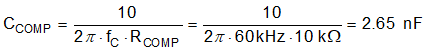
100 µF. Choose a standard value for RCOMP of 10 kΩ.
    Equation 43. GUID-B9CC6D00-43C5-4707-8519-4A3668A80FF5-low.gif
  2. To provide adequate phase boost at crossover while also allowing a fast settling time during a load or line transient, select CCOMP to place a zero at the higher of (1) one tenth of the crossover frequency, or (2) the load pole. Choose a standard value for CCOMP of 2.7 nF.
    Equation 44. GUID-B93D1F07-68BD-4C96-8FE0-DB15220A6D25-low.gif

    Such a low capacitance value also helps to avoid output voltage overshoot when recovering from dropout (when the input voltage is less than the output voltage setpoint and VCOMP is railed high).

  3. Calculate CHF to create a pole at the ESR zero and to attenuate high-frequency noise at COMP. CBW is the bandwidth-limiting capacitance of the error amplifier. CHF can not be significant enough to be necessary in some designs, like this one. CHF can be unpopulated, or used with a small 22 pF for more noise filtering.
    Equation 45. GUID-CEF638BE-68B2-423C-B771-4DFDB47D82B7-low.gif
Note:

Set a fast loop with high RCOMP and low CCOMP values to improve the response when recovering from operation in dropout.

For technical solutions, industry trends, and insights for designing and managing power supplies, please refer to TI's technical articles.