ZHCSNB5B June 2021 – February 2025 LM25148-Q1
PRODUCTION DATA
- 1
- 1 特性
- 2 应用
- 3 说明
- 4 说明(续)
- 5 可订购器件型号
- 6 引脚配置和功能
- 7 规格
-
8 详细说明
- 8.1 概述
- 8.2 功能方框图
- 8.3
特性说明
- 8.3.1 输入电压范围 (VIN)
- 8.3.2 高压偏置电源稳压器(VCC、VCCX、VDDA)
- 8.3.3 精密使能端 (EN)
- 8.3.4 电源正常监视器 (PG)
- 8.3.5 开关频率 (RT)
- 8.3.6 双随机展频 (DRSS)
- 8.3.7 软启动
- 8.3.8 输出电压设定值 (FB)
- 8.3.9 最短可控导通时间
- 8.3.10 误差放大器和 PWM 比较器(FB、EXTCOMP)
- 8.3.11 斜率补偿
- 8.3.12 电感器电流检测(ISNS+、VOUT)
- 8.3.13 断续模式电流限制
- 8.3.14 高侧和低侧栅极驱动器(HO、LO)
- 8.3.15 输出配置 (CNFG)
- 8.3.16 单输出双相运行
- 8.4 器件功能模式
- 9 应用和实施
- 10器件和文档支持
- 11修订历史记录
- 12机械、封装和可订购信息
8.3.3 精密使能端 (EN)
EN 引脚可以连接至高达 42V 的电压。LM25148-Q1 具有精密使能端。当 EN 电压大于 1V 时,会启用控制器切换。如果 EN 引脚被拉至 0.5V(典型值)以下,LM25148-Q1 会被关断,来自 VIN 的电流消耗 IQ 为 2.3μA(典型值)。当使能电压介于 0.5V 和 1V 之间时,LM25148-Q1 处于待机模式,此时 VCC 稳压器处于运行状态,但控制器不进行切换。在待机模式下,非开关输入静态电流典型值为 124μA。LM25148-Q1 的启用电压大于 1.0V。但是,许多应用都适合使用电阻分压器 RUV1 和 RUV2(如 图 8-2 中所示)来建立精密的 UVLO 电平。TI 不建议将 EN 引脚保持悬空。
在给定所需输入导通和关断电压的情况下,可以使用方程式 2 和方程式 3 来计算 UVLO 电阻。
方程式 2. 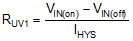
方程式 3. 
 图 8-2 可编程输入电压 UVLO 导通