ZHCSNB5B June 2021 – February 2025 LM25148-Q1
PRODUCTION DATA
- 1
- 1 特性
- 2 应用
- 3 说明
- 4 说明(续)
- 5 可订购器件型号
- 6 引脚配置和功能
- 7 规格
-
8 详细说明
- 8.1 概述
- 8.2 功能方框图
- 8.3
特性说明
- 8.3.1 输入电压范围 (VIN)
- 8.3.2 高压偏置电源稳压器(VCC、VCCX、VDDA)
- 8.3.3 精密使能端 (EN)
- 8.3.4 电源正常监视器 (PG)
- 8.3.5 开关频率 (RT)
- 8.3.6 双随机展频 (DRSS)
- 8.3.7 软启动
- 8.3.8 输出电压设定值 (FB)
- 8.3.9 最短可控导通时间
- 8.3.10 误差放大器和 PWM 比较器(FB、EXTCOMP)
- 8.3.11 斜率补偿
- 8.3.12 电感器电流检测(ISNS+、VOUT)
- 8.3.13 断续模式电流限制
- 8.3.14 高侧和低侧栅极驱动器(HO、LO)
- 8.3.15 输出配置 (CNFG)
- 8.3.16 单输出双相运行
- 8.4 器件功能模式
- 9 应用和实施
- 10器件和文档支持
- 11修订历史记录
- 12机械、封装和可订购信息
8.3.8 输出电压设定值 (FB)
在没有外部反馈电阻器的情况下,LM25148-Q1 稳压器输出可以独立配置为三个固定输出电压中的一个,或利用一个外部电阻分压器将输出调节至所需的电压。通过将 FB 直接连接到 VDDA,将输出设置为 3.3V。或者,通过分别在 FB 和 VDDA 之间安装 24.9kΩ 或 49.9kΩ 电阻器,将输出设置为 5V 或 12V。请参阅 表 8-1。
表 8-1 反馈配置电阻器
| 连接至 VDDA 的上拉电阻器 | VOUT 设定点 |
|---|---|
| 0Ω | 3.3V |
| 24.9kΩ | 5V |
| 49.9kΩ | 12V |
| 未安装 | 外部 FB 分压器设置 |
配置设置会被锁存并且无法更改,直到 LM25148-Q1 断电(且 VCC 电压降至其下降 UVLO 阈值以下),然后再次加电(VCC 上升到 3.4V 典型值以上)为止。或者,使用输出端与 AGND 之间连接的外部电阻分压器设置输出电压。输出电压调节范围为 0.8V 至 36V。FB 处的调节电压为 0.8V (VREF)。使用 方程式 6 分别计算上反馈电阻器和下反馈电阻器(分别用 RFB1 和 RFB2 表示)的值。
方程式 6. 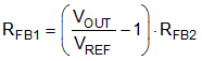
RFB2 的建议起始值为 10kΩ 至 20kΩ。
如果需要使用低 IQ 运行,则谨慎选择外部反馈电阻器。外部分压器的电流消耗会增加 LM25148-Q1 睡眠电流(典型值 9.5µA)。反射到 VIN 的分压器电流会按照 VOUT/VIN 的比率进行分压。