ZHCSHC3B january 2018 – june 2023 TPS61280D , TPS61280E , TPS61281D
PRODUCTION DATA
- 1
- 1 特性
- 2 应用
- 3 说明
- 4 Revision History
- 5 说明(续)
- 6 Device Comparison Table
- 7 Pin Configuration and Functions
- 8 Specifications
-
9 Detailed Description
- 9.1 Overview
- 9.2 Functional Block Diagram
- 9.3 Feature Description
- 9.4 Device Functional Modes
- 9.5 Programming
- 9.6
Register Maps
- 9.6.1 Slave Address Byte
- 9.6.2 Register Address Byte
- 9.6.3 I2C Registers, E2PROM, Write Protect
- 9.6.4 E2PROM Configuration Parameters
- 9.6.5 CONFIG Register [reset = 0x01]
- 9.6.6 VOUTFLOORSET Register [reset = 0x02]
- 9.6.7 VOUTROOFSET Register [reset = 0x03]
- 9.6.8 ILIMSET Register [reset = 0x04]
- 9.6.9 Status Register [reset = 0x05]
- 9.6.10 E2PROMCTRL Register [reset = 0xFF]
- 10Application and Implementation
- 11Power Supply Recommendations
- 12Layout
- 13Device and Documentation Support
- 14Mechanical, Packaging, and Orderable Information
9.4.4 Current Limit Operation
The TPS6128xD/E device features a valley inductor current limit scheme.
In dc/dc boost mode, the TPS6128xD/E device employs a current limit detection scheme in which the voltage drop across the synchronous rectifier is sensed during the off-time. In the TPS61280D the current limit threshold can be set via an I2C register. TPS6128xD/E devices have a fixed current limit threshold. See Section 6 for detailed information.
The output voltage is reduced as the power stage of the device operates in a constant current mode. The maximum continuous output current (IOUT(MAX)), before entering current limit (CL) operation, can be defined by Equation 6.
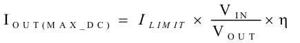
where
- η is the efficiency
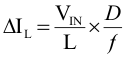
- The inductor peak-to-peak current ripple (ΔIL) is calculated by Equation 7
The output current, IOUT(DC), is the average of the rectifier ripple current waveform. When the load current is increased such that the trough is above the current limit threshold, the off-time is increased to allow the current to decrease to this threshold before the next on-time begins (so called frequency fold-back mechanism). When the current limit is reached the output voltage decreases during further load increase.
Figure 9-5 illustrates the inductor and rectifier current waveforms during current limit operation.
") Figure 9-5 Inductor/Rectifier Currents in Current Limit Operation (DC/DC Boost Mode)
Figure 9-5 Inductor/Rectifier Currents in Current Limit Operation (DC/DC Boost Mode)During pass-through mode, the TPS6128xD/E device is short-circuit protected by a very fast current limit detection scheme. If the current in the bypass FET exceeds approximately 7.5Amps a fault is declared and the device cycles through a start-up procedure.