ZHCSHC3B january 2018 – june 2023 TPS61280D , TPS61280E , TPS61281D
PRODUCTION DATA
- 1
- 1 特性
- 2 应用
- 3 说明
- 4 Revision History
- 5 说明(续)
- 6 Device Comparison Table
- 7 Pin Configuration and Functions
- 8 Specifications
-
9 Detailed Description
- 9.1 Overview
- 9.2 Functional Block Diagram
- 9.3 Feature Description
- 9.4 Device Functional Modes
- 9.5 Programming
- 9.6
Register Maps
- 9.6.1 Slave Address Byte
- 9.6.2 Register Address Byte
- 9.6.3 I2C Registers, E2PROM, Write Protect
- 9.6.4 E2PROM Configuration Parameters
- 9.6.5 CONFIG Register [reset = 0x01]
- 9.6.6 VOUTFLOORSET Register [reset = 0x02]
- 9.6.7 VOUTROOFSET Register [reset = 0x03]
- 9.6.8 ILIMSET Register [reset = 0x04]
- 9.6.9 Status Register [reset = 0x05]
- 9.6.10 E2PROMCTRL Register [reset = 0xFF]
- 10Application and Implementation
- 11Power Supply Recommendations
- 12Layout
- 13Device and Documentation Support
- 14Mechanical, Packaging, and Orderable Information
9.3.2 Spread Spectrum, PWM Frequency Dithering
The goal is to spread out the emitted RF energy over a larger frequency range so that the resulting EMI is similar to white noise. The end result is a spectrum that is continuous and lower in peak amplitude, making it easier to comply with electromagnetic interference (EMI) standards and with the power supply ripple requirements in cellular and non-cellular wireless applications. Radio receivers are typically susceptible to narrowband noise that is focused on specific frequencies.
Switching regulators can be particularly troublesome in applications where electromagnetic interference (EMI) is a concern. Switching regulators operate on a cycle-by-cycle basis to transfer power to an output. In most cases, the frequency of operation is either fixed or regulated, based on the output load. This method of conversion creates large components of noise at the frequency of operation (fundamental) and multiples of the operating frequency (harmonics).
The spread spectrum architecture varies the switching frequency by ca. ±15% of the nominal switching frequency thereby significantly reducing the peak radiated and conducting noise on both the input and output supplies. The frequency dithering scheme is modulated with a triangle profile and a modulation frequency fm.
 Figure 9-1 Spectrum of a Frequency Modulated Sin. Wave with Sinusoidal Variation in Time
 copyright IEEE TRANSACTIONS ON ELECTROMAGNETIC COMPATIBILITY, VOL. 47, NO.3, AUGUST 2005.") Figure 9-2 Spread Bands of Harmonics in Modulated Square Signals (1)
Figure 9-2 Spread Bands of Harmonics in Modulated Square Signals (1)The above figures show that after modulation the sideband harmonic is attenuated compared to the non-modulated harmonic, and the harmonic energy is spread into a certain frequency band. The higher the modulation index (mf) the larger the attenuation.
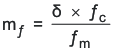
where
- fc is the carrier frequency (approx. 2.3MHz)
- fm is the modulating frequency (approx. 40kHz)
- δ is the modulation ratio (approx 0.15)

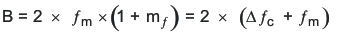
The maximum switching frequency fc is limited by the process and finally the parameter modulation ratio (δ), together with fm, which is the side-band harmonics bandwidth around the carrier frequency fc. The bandwidth of a frequency modulated waveform is approximately given by the Carson’s rule and can be summarized as:
fm < RBW: The receiver is not able to distinguish individual side-band harmonics, so, several harmonics are added in the input filter and the measured value is higher than expected in theoretical calculations.
fm > RBW: The receiver is able to properly measure each individual side-band harmonic separately, so the measurements match with the theoretical calculations.