ZHCSHC3B january 2018 – june 2023 TPS61280D , TPS61280E , TPS61281D
PRODUCTION DATA
- 1
- 1 特性
- 2 应用
- 3 说明
- 4 Revision History
- 5 说明(续)
- 6 Device Comparison Table
- 7 Pin Configuration and Functions
- 8 Specifications
-
9 Detailed Description
- 9.1 Overview
- 9.2 Functional Block Diagram
- 9.3 Feature Description
- 9.4 Device Functional Modes
- 9.5 Programming
- 9.6
Register Maps
- 9.6.1 Slave Address Byte
- 9.6.2 Register Address Byte
- 9.6.3 I2C Registers, E2PROM, Write Protect
- 9.6.4 E2PROM Configuration Parameters
- 9.6.5 CONFIG Register [reset = 0x01]
- 9.6.6 VOUTFLOORSET Register [reset = 0x02]
- 9.6.7 VOUTROOFSET Register [reset = 0x03]
- 9.6.8 ILIMSET Register [reset = 0x04]
- 9.6.9 Status Register [reset = 0x05]
- 9.6.10 E2PROMCTRL Register [reset = 0xFF]
- 10Application and Implementation
- 11Power Supply Recommendations
- 12Layout
- 13Device and Documentation Support
- 14Mechanical, Packaging, and Orderable Information
10.2.1.2.1 Inductor Selection
A boost converter normally requires two main passive components for storing energy during the conversion, an inductor and an output capacitor are required. It is advisable to select an inductor with a saturation current rating higher than the possible peak current flowing through the power switches.
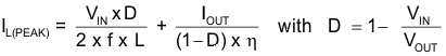
The inductor peak current varies as a function of the load, the input and output voltages and can be estimated using Equation 8.
Selecting an inductor with insufficient saturation performance can lead to excessive peak current in the converter. This could eventually harm the device and reduce it's reliability.
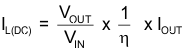
When selecting the inductor, as well as the inductance, parameters of importance are: maximum current rating, series resistance, and operating temperature. The inductor DC current rating should be greater than the maximum input average current, refer to Equation 9 and the Section 9.4.4 section for more details.
The TPS6128xD series of step-up converters have been optimized to operate with a effective inductance in the range of 200 nH to 800 nH. Larger or smaller inductor values can be used to optimize the performance of the device for specific operating conditions. For more details, see the Section 10.2.1.2.4 section.
In high-frequency converter applications, the efficiency is essentially affected by the inductor AC resistance (that is, quality factor) and to a smaller extent by the inductor DCR value. To achieve high efficiency operation, care should be taken in selecting inductors featuring a quality factor above 25 at the switching frequency. Increasing the inductor value produces lower RMS currents, but degrades transient response. For a given physical inductor size, increased inductance usually results in an inductor with lower saturation current.
The total losses of the coil consist of both the losses in the DC resistance, R(DC) , and the following frequency-dependent components:
- The losses in the core material (magnetic hysteresis loss, especially at high switching frequencies)
- Additional losses in the conductor from the skin effect (current displacement at high frequencies)
- Magnetic field losses of the neighboring windings (proximity effect)
- Radiation losses
For good efficiency, the inductor DC resistance should be less than 30 mΩ. The following inductor series from different suppliers have been used with the TPS6128xD converters.
| SERIES | DIMENSIONS (in mm) | DC INPUT CURRENT LIMIT SETTING |
|---|---|---|
| DFE252010C | 2.5 x 2.0 x 1.0 max. height | ≤3000 mA |
| DFE252012C | 2.5 x 2.0 x 1.2 max. height | ≤3500 mA |
| DFR252010C | 2.5 x 2.0 x 1.0 max. height | ≤3000 mA |
| DFE252012C | 2.5 x 2.0 x 1.2 max. height | ≤3500 mA |
| DFE252012P | 2.5 x 2.0 x 1.2 max. height | ≤3500 mA |
| DFE201610C | 2.0 x 1.6 x 1.0 max. height | ≤2000 mA |
| DFE201612C | 2.0 x 1.6 x 1.2 max. height | ≤3000 mA |
| DFE201612P | 2.0 x 1.6 x 1.2 max. height | ≤3000 mA |