ZHCSHC3B january 2018 – june 2023 TPS61280D , TPS61280E , TPS61281D
PRODUCTION DATA
- 1
- 1 特性
- 2 应用
- 3 说明
- 4 Revision History
- 5 说明(续)
- 6 Device Comparison Table
- 7 Pin Configuration and Functions
- 8 Specifications
-
9 Detailed Description
- 9.1 Overview
- 9.2 Functional Block Diagram
- 9.3 Feature Description
- 9.4 Device Functional Modes
- 9.5 Programming
- 9.6
Register Maps
- 9.6.1 Slave Address Byte
- 9.6.2 Register Address Byte
- 9.6.3 I2C Registers, E2PROM, Write Protect
- 9.6.4 E2PROM Configuration Parameters
- 9.6.5 CONFIG Register [reset = 0x01]
- 9.6.6 VOUTFLOORSET Register [reset = 0x02]
- 9.6.7 VOUTROOFSET Register [reset = 0x03]
- 9.6.8 ILIMSET Register [reset = 0x04]
- 9.6.9 Status Register [reset = 0x05]
- 9.6.10 E2PROMCTRL Register [reset = 0xFF]
- 10Application and Implementation
- 11Power Supply Recommendations
- 12Layout
- 13Device and Documentation Support
- 14Mechanical, Packaging, and Orderable Information
9.4.2 Pass-Through Mode
The TPS6128xD/E contains an internal switch for bypassing the dc/dc boost converter during pass-through mode. When the input voltage is larger than the preset output voltage, the converter seamlessly transitions into 0% duty cycle operation and the bypass FET is fully enhanced. Entry in pass-through mode is triggered by condition where VOUT >(1+2%)* VOUT_NORM and no switching has occurred during past 8µs.
In this mode of operation, the load (2G RF PA for instance) is directly supplied from the battery for maximum RF output power, highest efficiency and lowest possible input-to-output voltage difference. The device consumes only a standby current of 15µA (typ). In pass-through mode, the device is short-circuit protected by a very fast current limit detection scheme.
During this operation, the output voltage follows the input voltage and will not fall below the programmed output voltage threshold as the input voltage decreases. The output voltage drop during pass-through mode depends on the load current and input voltage, the resulting output voltage is calculated as:
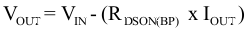
Conversely, the efficiency in pass-through mode is defined as:
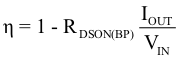
- in which RDSON(BP) is the typical on-resistance of the bypass FET
 Figure 9-4 DC Output Voltage vs. Input Voltage
Pass-through mode exit is triggered when the output voltage reaches the pre-defined threshold (that is, 3.4V).
During pass-through mode, the TPS6128xD/E device is short-circuit protected by a fast current limit detection scheme. If the current in the pass-through FET exceeds approximately 7.3 Amps a fault is declared and the device cycles through a start-up procedure.