ZHCSGM4C August 2017 – October 2023 OPA838
PRODUCTION DATA
- 1
- 1 特性
- 2 应用
- 3 说明
- 4 Revision History
- 5 Device Comparison Table
- 6 Pin Configuration and Functions
-
7 Specifications
- 7.1 Absolute Maximum Ratings
- 7.2 ESD Ratings
- 7.3 Recommended Operating Conditions
- 7.4 Thermal Information
- 7.5 Electrical Characteristics: VS = 5 V
- 7.6 Electrical Characteristics: VS = 3 V
- 7.7 Typical Characteristics: VS = 5 V
- 7.8 Typical Characteristics: VS = 3 V
- 7.9 Typical Characteristics: Over Supply Range
- 8 Detailed Description
- 9 Application and Implementation
- 10Device and Documentation Support
- Mechanical, Packaging, and Orderable Information
封装选项
机械数据 (封装 | 引脚)
散热焊盘机械数据 (封装 | 引脚)
订购信息
9.1.4 Output Noise Calculations
The decompensated voltage feedback of the OPA838 op amp offers among the lowest input voltage and current noise terms for any device with a supply current less than 1 mA. Figure 9-3 shows the op amp noise analysis model that includes all noise terms. In this model, all the noise terms are shown as noise voltage or current density terms in nV/√Hz or pA/√Hz.
 Figure 9-3 Op-Amp Noise-Analysis
Model
Figure 9-3 Op-Amp Noise-Analysis
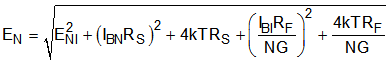
ModelThe total output spot noise voltage is computed as the square root of the squared contributing terms to the output noise voltage. This computation is adding all the contributing noise powers at the output by superposition, then taking the square root to return to a spot noise voltage. Equation 3 shows the general form for this output noise voltage using the terms presented in Figure 9-3.

Dividing this expression by the noise gain (NG = 1 + RF / RG) gives the equivalent input-referred spot noise voltage at the noninverting input, as shown in Equation 4.
Using the resistor values shown in Table 9-1 with RS = 0 Ω results in a constant input-referred voltage noise of 2.86 nV/√Hz. Reducing the resistor values brings this number closer to the intrinsic 1.9 nV/√Hz of the OPA838. Adding RS for bias current cancellation in noninverting mode adds the noise from RS to the total output noise; see Equation 3. In inverting mode, bypass the RS bias-current cancellation resistor with a capacitor for the best noise performance.