ZHCSGM4C August 2017 – October 2023 OPA838
PRODUCTION DATA
- 1
- 1 特性
- 2 应用
- 3 说明
- 4 Revision History
- 5 Device Comparison Table
- 6 Pin Configuration and Functions
-
7 Specifications
- 7.1 Absolute Maximum Ratings
- 7.2 ESD Ratings
- 7.3 Recommended Operating Conditions
- 7.4 Thermal Information
- 7.5 Electrical Characteristics: VS = 5 V
- 7.6 Electrical Characteristics: VS = 3 V
- 7.7 Typical Characteristics: VS = 5 V
- 7.8 Typical Characteristics: VS = 3 V
- 7.9 Typical Characteristics: Over Supply Range
- 8 Detailed Description
- 9 Application and Implementation
- 10Device and Documentation Support
- Mechanical, Packaging, and Orderable Information
封装选项
机械数据 (封装 | 引脚)
散热焊盘机械数据 (封装 | 引脚)
订购信息
9.2.2.2 Detailed Design Procedure
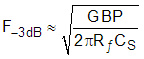
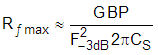
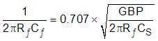
The primary design requirement is to set the achievable transimpedance gain and compensate the operational amplifier with CF for the desired response shape. A detailed transimpedance design methodology is available in Transimpedance Considerations for High-Speed Amplifiers. With a source capacitance set and the amplifier selected to provide a particular gain bandwidth product, the achievable transimpedance gain and resulting Butterworth bandwidth are tightly coupled as Equation 5 illustrates. Use Equation 6 to solve for a maximum RF value. When the RF is selected, the feedback pole is set by Equation 7 to be at 0.707 of the characteristic frequency. At that compensation point, the closed-loop bandwidth is that characteristic frequency with a Butterworth response.
- With the 100-pF source capacitance, 300-MHz gain bandwidth product, and the 2.2-MHz closed-loop bandwidth target in the transimpedance stage, solve Equation 6 for a maximum gain of 100 kΩ.
- Set the feedback pole at 0.707 times that 2.2-MHz Butterworth bandwidth. This sets the target 1 / (2π × R F × CF) = 1.55 MHz. Solving for CF sets the target to 1 pF
- If dc precision is desired, add a 100-kΩ resistor to ground on the noninverting input. If DC precision is not required, ground the noninverting input
- Add a resistor noise filtering capacitor in parallel with the 100-kΩ resistor.
- Add a small series resistor isolating this capacitor from the noninverting input.
- Select a final filter capacitor for the load. (In this example, a value of 2.2 nF is used as a typical SAR input capacitor.)
- Add a series resistor to the final filter capacitor to form a 1-MHz pole. In this example, that is 73.2 Ω.
- Confirm this resistor is greater than the minimum recommended value illustrated in Figure 7-49.
Implementing this design and simulating the performance using the TINA model for the response to the output pin and to the final capacitive load shows the expected results of Figure 9-8. Here, the exact 2.2-MHz flat Butterworth response to the output pin is shown with the final single pole rolloff at 1 MHz at the final 2.2-nF capacitor.