ZHCSGM4C August 2017 – October 2023 OPA838
PRODUCTION DATA
- 1
- 1 特性
- 2 应用
- 3 说明
- 4 Revision History
- 5 Device Comparison Table
- 6 Pin Configuration and Functions
-
7 Specifications
- 7.1 Absolute Maximum Ratings
- 7.2 ESD Ratings
- 7.3 Recommended Operating Conditions
- 7.4 Thermal Information
- 7.5 Electrical Characteristics: VS = 5 V
- 7.6 Electrical Characteristics: VS = 3 V
- 7.7 Typical Characteristics: VS = 5 V
- 7.8 Typical Characteristics: VS = 3 V
- 7.9 Typical Characteristics: Over Supply Range
- 8 Detailed Description
- 9 Application and Implementation
- 10Device and Documentation Support
- Mechanical, Packaging, and Orderable Information
封装选项
机械数据 (封装 | 引脚)
散热焊盘机械数据 (封装 | 引脚)
订购信息
8.3.4 Trade-Offs in Selecting The Feedback Resistor Value
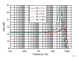
The OPA838 is specified using a 1-kΩ feedback resistor with a 200-Ω gain resistor to ground in a noninverting gain of 6 V/V configuration. These values give a good compromise, keeping the noise contribution of the resistors well below that of the amplifier noise terms and minimal power in the feedback network as the output voltage swing creates load current back into the feedback network. Decreasing these values improves the noise at the cost of more power dissipated in the feedback network. Low values increase the harmonic distortion as the feedback load decreases. Increasing the RF value at a particular gain increases the output noise contribution of those resistors possibly becoming dominant. As the feedback resistor values continue to increase (and the RG at a fixed target gain), there is a loss of phase margin as the impedance that drives the inverting input capacitance brings in an added loop pole at lower frequencies. Figure 8-3 shows this at a gain of 6 V/V with increasing RF values. This noninverting test shows more peaking as the RF values increase due to the 1-pF
common-mode input capacitance at the inverting input. The TINA simulation model gives excellent prediction of these effects.
 Figure 8-3 Frequency Response With Various Feedback Resistor Values
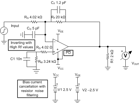
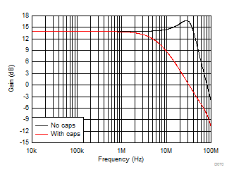
Operating the OPA838 in inverting mode with higher RF values increases response peaking due to the loss of phase margin effect. In the inverting case, a pair of capacitors can flatten the response at the cost of lower closed-loop bandwidth. Figure 8-4 shows an example with a 20-kΩ RF value at an inverting gain of –5 V/V (noise gain = 6 V/V) with optional capacitors (CF and CG). Figure 8-4 shows optional bias current cancellation elements on the noninverting input. The total resistance value matches the parallel combination of RG || RF, which reduces the DC output error term due to bias current to IOS × RF. The 10-nF capacitor is added across the larger part of this bias current canceling resistance to filter noise and the 20 Ω is split out to isolate the capacitor self resonance from the noninverting input. Figure 8-5 illustrates the small-signal response shape with and without these capacitors. The feedback capacitor (CF), is selected to set a desired closed-loop bandwidth with RF. CG is added to ground to shape the noise gain up over frequency to be greater than or equal to 6 V/V at higher frequencies. In this example, that higher frequency noise gain is 1 + 6 / 1.2 = 6 V/V, adding the 1-pF device common-mode capacitance to the external 5 pF. Using the capacitors to set the feedback ratio removes the pole produced in the feedback driving from purely resistive source to the inverting parasitic capacitance.
 Figure 8-4 G = –5 V/V With Optional Compensation
 Figure 8-5 Inverting Response With and Without Compensation