SPRACY3 June 2021 F29H850TU , F29H859TU-Q1 , F29P329SM-Q1 , TMS320F280023C , TMS320F280025C , TMS320F280025C-Q1 , TMS320F280040C-Q1 , TMS320F280041C , TMS320F280041C-Q1 , TMS320F280048C-Q1 , TMS320F280049C , TMS320F280049C-Q1 , TMS320F28076 , TMS320F28379D , TMS320F28379D-Q1 , TMS320F28379S , TMS320F28386D , TMS320F28386D-Q1 , TMS320F28386S , TMS320F28386S-Q1 , TMS320F28388D , TMS320F28388S , TMS320F28P650DH , TMS320F28P650DK , TMS320F28P650SH , TMS320F28P650SK , TMS320F28P659DH-Q1 , TMS320F28P659DK-Q1 , TMS320F28P659SH-Q1
3.3 CLB Output
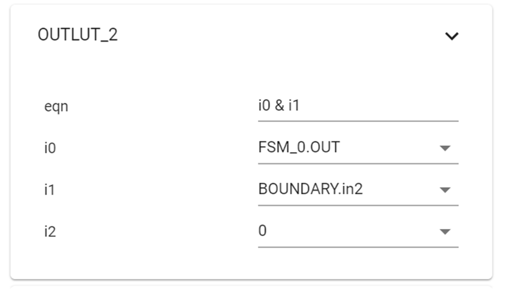
The final step is to use the output LUT block to combine the FSM_OUT and original EPWM1B’ with AND logic. According to the Table 3-2, OUTPUT LUT2_0 of CLB TILE1 is used to route the resulting output (FSM_OUT&EPWM1B’) as the new EPWM1B, as shown in Figure 3-4. Likewise, OUTPUT LUT2_0 of CLB TILE2 is used for EPWM2B. That is why two CLB TILEs are required in this application.
| CLB Instance | CLB Output Signal | Peripheral Signal | Peripheral Name |
|---|---|---|---|
| CBL1 | CLB1_OUT0_0 | PWMA | EPWM1 |
| CBL1 | CLB1_OUT1_0 | PWMA_OE | EPWM1 |
| CBL1 | CLB1_OUT2_0 | PWMB | EPWM1 |
| CBL1 | CLB1_OUT3_0 | PWMB_OE | EPWM1 |
| CBL1 | CLB1_OUT4_0 | AQ_PWMA | EPWM1 |
| CBL1 | CLB1_OUT5_0 | AQ_PWMB | EPWM1 |
| CBL1 | CLB1_OUT6_0 | DB_PWMA | EPWM1 |
| CBL1 | CLB1_OUT7_0 | DB_PWMB | EPWM1 |
| CBL1 | CLB1_OUT0_1 | QA | EQEP1 |
| CBL1 | CLB1_OUT1_1 | QB | EQEP1 |
| CBL1 | CLB1_OUT2_1 | DDIR | EQEP1 |
| CBL1 | CLB1_OUT3_1 | QCLK | EQEP1 |
| CBL1 | CLB1_OUT4_1 | G1.2 | CLB X BAR |
| CBL1 | CLB1_OUT5_1 | G3.2 | CLB X BAR |
 Figure 3-4 OUTPUT LUT2_0 Configuration
 As shown in Table 3-2, each CLB output signal passes through an external multiplexer that intersects a specific peripheral signal. Thus, to export the CLB output to the original EPWM1B pin (GPIO1 in the example), it is needed to enable the OUTPUT LUT2_0 using the OUT_EN register, as shown in the below code snippets.
CLB_setOutputMask(CLB1_BASE, 0x4, true);   //1<<2 out2

CLB_setOutputMask(CLB2_BASE, 0x4, true);  //1<<2 out2