SPRACY3 June 2021 F29H850TU , F29H859TU-Q1 , F29P329SM-Q1 , TMS320F280023C , TMS320F280025C , TMS320F280025C-Q1 , TMS320F280040C-Q1 , TMS320F280041C , TMS320F280041C-Q1 , TMS320F280048C-Q1 , TMS320F280049C , TMS320F280049C-Q1 , TMS320F28076 , TMS320F28379D , TMS320F28379D-Q1 , TMS320F28379S , TMS320F28386D , TMS320F28386D-Q1 , TMS320F28386S , TMS320F28386S-Q1 , TMS320F28388D , TMS320F28388S , TMS320F28P650DH , TMS320F28P650DK , TMS320F28P650SH , TMS320F28P650SK , TMS320F28P659DH-Q1 , TMS320F28P659DK-Q1 , TMS320F28P659SH-Q1
3.2 Counter and FSM Configuration
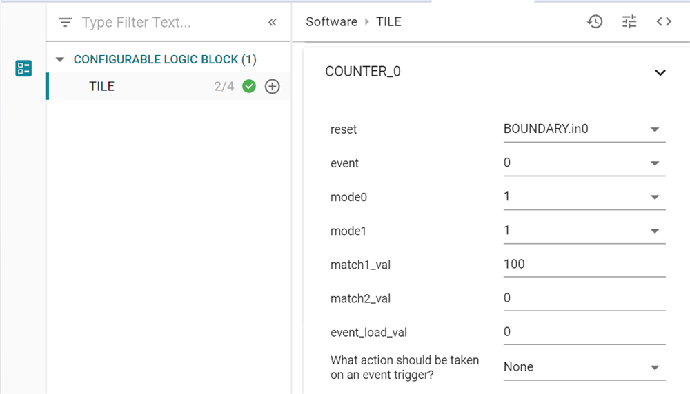
The counter block is used to achieve the customized delay. Since the counter will always reset to 0 if the “Reset” input remains high, the trip signal, which is active low, can be used to trigger the counter to start counting. Thus, both MODE_0 and MODE_1 can be set to 1, which enables the counter increment as soon as the trip signal goes low. MATCH1 is set with the expected delay value, like 100, which means 1 μs, with the time base of 100 MHz for CLB module. Figure 3-1 shows how the counter is configured in the GUI-based SysConfig tool.
 Figure 3-1 Counter Settings in the
SysConfig
Figure 3-1 Counter Settings in the
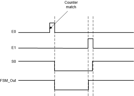
SysConfigThe state machine has been implemented with the FSW block as shown in Figure 3-2. Two inputs are used to identify the state of S0. E0 is referred to the counter match event, while E1 is the rising edge of the trip signal. Thus, S0 will go down at E0 and rise at E1. Thus, the Karnaugh map can be created for S0 state, as given in Table 3-1.
 Figure 3-2 State Machine in the FSW
Block
Figure 3-2 State Machine in the FSW
Block| S0 | E0E1 | 00 | 01 | 11 | 10 |
|---|---|---|---|---|---|
| 0 | 0 | 1 | 1 | 0 | |
| 1 | 1 | 1 | 0 | 0 |
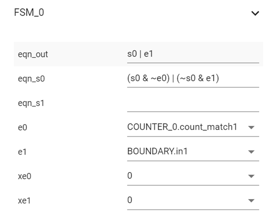
Based on the Karnaugh map, the FSM equations for S0 can be deduced as shown in Equation 1.
Since the state transitions will always take 1 clock cycle to take effect, in order to reduce the undesirable delay, the FSM output takes the combinational output of S0 and E1, that is shown in Equation 2.
 Figure 3-3 FSM Configuration