SPRACY3 June 2021 F29H850TU , F29H859TU-Q1 , F29P329SM-Q1 , TMS320F280023C , TMS320F280025C , TMS320F280025C-Q1 , TMS320F280040C-Q1 , TMS320F280041C , TMS320F280041C-Q1 , TMS320F280048C-Q1 , TMS320F280049C , TMS320F280049C-Q1 , TMS320F28076 , TMS320F28379D , TMS320F28379D-Q1 , TMS320F28379S , TMS320F28386D , TMS320F28386D-Q1 , TMS320F28386S , TMS320F28386S-Q1 , TMS320F28388D , TMS320F28388S , TMS320F28P650DH , TMS320F28P650DK , TMS320F28P650SH , TMS320F28P650SK , TMS320F28P659DH-Q1 , TMS320F28P659DK-Q1 , TMS320F28P659SH-Q1
5.3 Achieve 2 Level Protection Scheme
In actual applications, there are some non-serious events that require only the outer switches to turn off and keep the normal operation for inner switches. Thus, the two level protection scheme is needed:
- 1st level protection: only require the outer switch (S1/S4) to shut down, S2/S3 keep normal operation
- 2nd level protection: outer switch (S1/S4) to be switched off immediately, inner switch (S2/S3) should be turned off after a defined delay
From the above point of view, 1st level protection will normally occurs before 2nd level one, with the trip trigger level lower for 1st level protection, but during the sudden over current or short circuit conditions, these two protection events might occur almost at the same time. Therefore, in either protection trigger event, the EPWM for the outer switch is required to achieve CBC protection. To simply the configuration, the two trip events can be logically OR to serve as the same source for the CBC protection. According to the ePWM X-BAR architecture, the muxes that are enabled will be intrinsically OR’d before being passed on to the respective TRIPx signal on the EPWM. If using two GPIO pins for the external protection signals, two Input X-BAR INPUTs are selected for the same TRIP source.
    // Configure INPUT X-BAR 1 as EPWM X-BAR TRIP 4 source
    XBAR_setEPWMMuxConfig(XBAR_TRIP4,XBAR_EPWM_MUX01_INPUTXBAR1);
    XBAR_enableEPWMMux(XBAR_TRIP4, XBAR_MUX01);
    // Configure INPUT X-BAR 2 as EPWM X-BAR TRIP 4 source
    XBAR_setEPWMMuxConfig(XBAR_TRIP4,XBAR_EPWM_MUX03_INPUTXBAR2);
    XBAR_enableEPWMMux(XBAR_TRIP4, XBAR_MUX03);
Note that the trip signals should change to active high with the OR logic implemented. Actually, there can be no change for the external protection circuits if designed with active low initially. Using GPxINV in GPIO register configurations can inverse the IO pin logic.
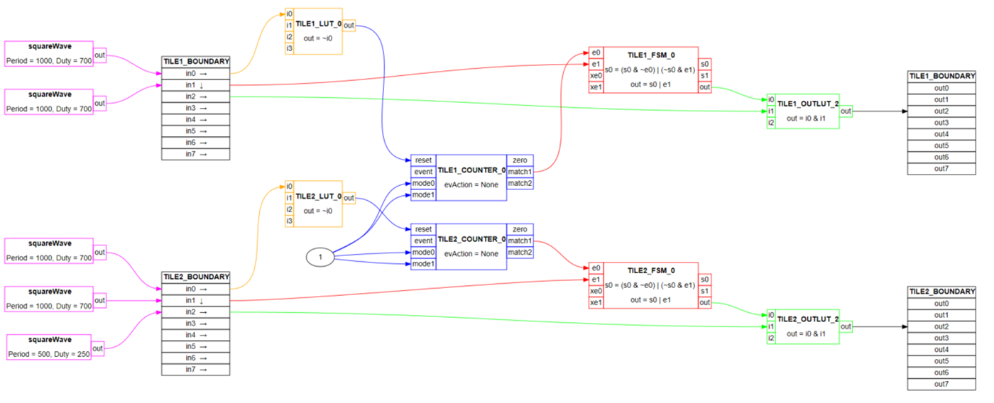
Besides, the method discussed in Section 3 is still applied for 2nd level protection, where the 2nd level trip event is selected as the CLB input for the delayed protection. However, different from Section 3.1, it is the falling edge of the trip signal that used to determine the rising moment of the expected CLB signal. Thus the completed design block diagrams should be modified as Figure 5-2.
 Figure 5-2 Completed Design Block Diagrams
for 2 Level Protection Scheme
Figure 5-2 Completed Design Block Diagrams
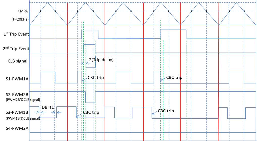
for 2 Level Protection SchemeTherefore, the expected EPWM protection logic with CLB in Figure 5-2 should be updated as shown in Figure 5-3.
 Figure 5-3 Updated EPWM Protection Logic With
CLB for 2 Level Protection Scheme
Figure 5-3 Updated EPWM Protection Logic With
CLB for 2 Level Protection SchemeAs mentioned in Section 5.1, it is also possible to use internal CMPSS for the two level protection scheme, with the same sensing signal. Since there are two comparators with one CMPSS, including CMPH and CMPL, which can provide trigger signals for the two trip events, with two different references.
   CMPSS_setDACValueHigh(CMPSS1_BASE, trip_point_2);
     CMPSS_setDACValueLow(CMPSS1_BASE, trip_point_1);

    // Configure CMPSS1_CTRIPH as EPWM X-BAR TRIP 4 source
    XBAR_setEPWMMuxConfig(XBAR_TRIP4,XBAR_EPWM_MUX00_CMPSS1_CTRIPH);
    XBAR_enableEPWMMux(XBAR_TRIP4, XBAR_MUX00);
    // Configure CMPSS1_CTRIPL as EPWM X-BAR TRIP 4 source
    XBAR_setEPWMMuxConfig(XBAR_TRIP4,XBAR_EPWM_MUX01_CMPSS1_CTRIPL);
    XBAR_enableEPWMMux(XBAR_TRIP4, XBAR_MUX01);