SLWU079D March 2012 – April 2016
-
TSW140x High Speed Data Capture/Pattern Generator Card
- Trademarks
- 1 Functionality
- 2 Hardware Configuration
- 3 Software Start up
- 4 ADC Data Capture Software Operation
- 5 TSW1400 Pattern Generator Operation
- 6 TSW1405 Functional Description
- 7 TSW1406 Functional Description
- 8 Revision History
1 Functionality
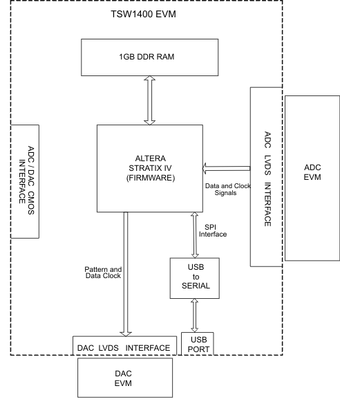
The TSW1400 has two direct interfaces to TI ADC EVMs. One option captures data through a LVDS interface and the other uses a CMOS interface. Sampled data from the ADC is de-serialized and formatted by an Altera Stratix IV FPGA, then stored into an external onboard 1GByte DDR memory card. The onboard memory enables the TSW1400 to store up to 512M 16 bit data samples. To acquire data on a host PC, the FPGA reads the data from memory and transmits it on Serial Peripheral Interface (SPI). An onboard high speed USB to SPI converter bridges the FPGA SPI interface to the host PC and GUI.
The TSW1400 has two direct interfaces to TI DAC EVMs. In Pattern Generator Mode, the TSW1400 generates desired test patterns for DAC EVMs under test. These patterns are sent from the host PC over the USB interface to the TSW1400. The FPGA stores the data received into the board DDR memory module. The data from the memory is then read by the FPGA and transmitted to a DAC EVM either across a DAC LVDS interface connector or a CMOS interface connector.
A block diagram of the TSW1400 EVM is shown in Figure 1.
 Figure 1. TSW1400EVM Block Diagram