SCAA124 April 2015 RM41L232 , RM42L432 , RM44L520 , RM44L920 , RM46L430 , RM46L440 , RM46L450 , RM46L830 , RM46L840 , RM46L850 , RM46L852 , RM48L530 , RM48L540 , RM48L730 , RM48L740 , RM48L940 , RM48L950 , RM48L952 , RM57L843 , TMS570LC4357 , TMS570LC4357-EP , TMS570LC4357-SEP , TMS570LS0232 , TMS570LS0332 , TMS570LS0432 , TMS570LS0714 , TMS570LS0714-S , TMS570LS0914 , TMS570LS1114 , TMS570LS1115 , TMS570LS1224 , TMS570LS1225 , TMS570LS1227 , TMS570LS2124 , TMS570LS2125 , TMS570LS2134 , TMS570LS2135 , TMS570LS3134 , TMS570LS3135 , TMS570LS3137
2.5.2 Stressing Special Pins
Analog and mixed signal products may have a combination of pin functions that require some pins to be treated as digital pins and others as analog pins. Generally, the analog pins will have only one bias setting to function properly, so, there is one stress to perform on those types of pins. The digital pins can have vectors and clocks and must be treated as described in JESD78. Analog and mixed signal products can also have special function pins that can be difficult to know how to stress. Examples of special pins may be LDO, PWM, BOOT, PHASE, HB, VCC and others. In general, these pins provide a bias to other pins on the same product or help regulate the product’s operation or provide bias to other devices. There is considerable debate on how to stress these pins. Some would like to test these pins as they are configured in a normal application. Others want to stress them as either outputs as power supplies or inputs as power supplies. A JESD78 Latch-Up Sub-Team is working on the resolving this issue; the results of this team’s activity will be in a future revision of the standard.
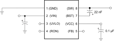
In this example, using a voltage regulator, Figure 7 shows a set-up that treats these pins as if they were in a common application setting.
 Figure 7. Typical Voltage Regulator Application Set-Up for Latch-Up Stress
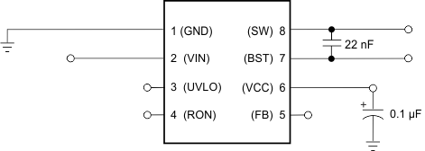
  Figure 8. Typical Voltage Regulator Set-Up for Latch-Up Stress
 There are two pins that may have more than one way to be stressed: pins 6 and 7. Each, in the application, provides a bias or control charge flow to another pin or provide internal regulation support. One could stress both pins without the capacitors but categorizing them into a group may be difficult. Pin 6 provides a bias, is it a power supply or output? Pin 7 provides charge control to pin 8, is it an output or power supply? Additionally, Pin 7 must always be within a small voltage above Pin 8. Each category could be applied (see Figure 8). If each is an output then the pins would receive both a positive and negative current pulse since output can fluctuate between positive and negative values. Both pins can be labeled as power supplies and biased to a correct value. If this is the case then an over-voltage pulse will be applied. In many scenarios, neither of these configurations will work. Knowledge of the circuitry supporting the pin of interest will be important in assigning the proper stress type. Generally, avoidance of an unstable condition is paramount. If stability is not achieved, the results are not trustworthy. Engineering judgment may be necessary to properly exercise the pins.
Another option, described in Annex A of JESD78D, is to not directly stress these pins and have the capacitors in place particularly if the device is unstable during any other set-up. The over-voltage test on pin 2 would internally stress each of the externally unstressed pin(s). The part’s stability is generally very good with this type of set-up since Pin 7 and Pin 8 will maintain the required voltage separation. The remaining pins would be stressed as their descriptions require.