SCAA124 April 2015 RM41L232 , RM42L432 , RM44L520 , RM44L920 , RM46L430 , RM46L440 , RM46L450 , RM46L830 , RM46L840 , RM46L850 , RM46L852 , RM48L530 , RM48L540 , RM48L730 , RM48L740 , RM48L940 , RM48L950 , RM48L952 , RM57L843 , TMS570LC4357 , TMS570LC4357-EP , TMS570LC4357-SEP , TMS570LS0232 , TMS570LS0332 , TMS570LS0432 , TMS570LS0714 , TMS570LS0714-S , TMS570LS0914 , TMS570LS1114 , TMS570LS1115 , TMS570LS1224 , TMS570LS1225 , TMS570LS1227 , TMS570LS2124 , TMS570LS2125 , TMS570LS2134 , TMS570LS2135 , TMS570LS3134 , TMS570LS3135 , TMS570LS3137
2.5.3 High Voltage Testing
High voltage CMOS and BiCMOS devices can have some unique problems when Latch-Up stress is applied. In many cases MSV will have to be applied. Also in many of today’s high voltage products, there is little headroom above the data sheet VABSMAX to set the current stress voltage clamps without potentially causing a catastrophic failure. There may be cases under these conditions that VABSMAX may need to be used. There is also the consideration that most Latch-Up test equipment has a 100 V/1 A ceiling on their sourcing voltage and current. When confronted with this problem one can define the VMAX at a lower value and do the over-voltage and current pulse voltage clamps at the machine maximum voltage. Another possibility is to add external power supplies that reach the desired value and stress appropriately.
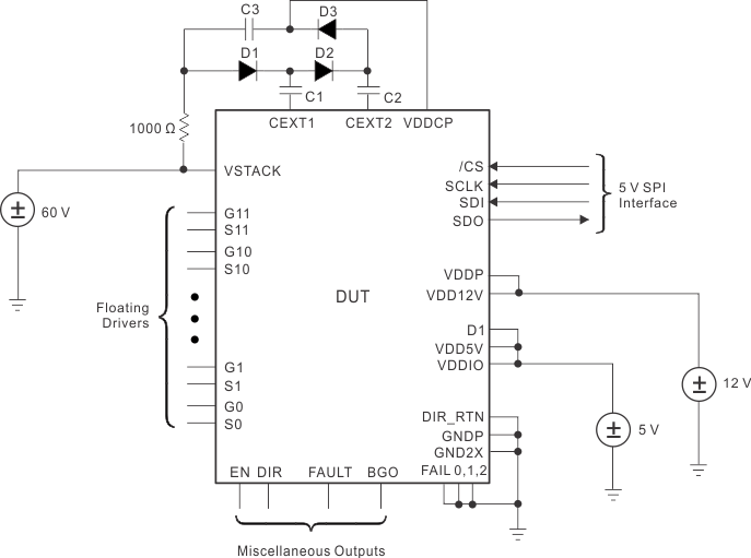
In the example shown in Figure 9, a mixed signal multi-port regulator is stressed using a combination of digital and analog methods. The product required vectors on the serial peripheral interface (SPI) to set the conditions of the drivers and the other outputs. This device also used charge pump drivers that, in the application, were controlled by a network of diodes, a resistor and capacitors to provide a bias to the charge pump pin. Any stress on these charge pump driver pins would cause the device to malfunction (become unstable). This is a closed network and susceptible only through other power supply variation. This network was not stressed during Latch-Up testing. All of the outputs and drivers were stressed both with positive and negative current pulses. The SPI clocked pins were not stressed for stability reasons. The overvoltage stress on the three power supplies was set for the 5 V supply at 1.5 x VMAX, the 12 V supply used an MSV of 1.2 x VMAX and the 60 V supply used an MSV of 1.1 x VMAX. Initial testing of this product found Latch-Up problems in the driver and sense pins which was understood and corrected. Upon retest the product passed all Latch-Up criteria.
 Figure 9. Product With Multiple Regulators Controlled by SPI